Resistor with improved switchable resistance and non-volatile memory device
a resistor and switchable resistance technology, applied in semiconductor devices, semiconductor/solid-state device details, electrical apparatus, etc., can solve the problems of time-consuming and hardly reproducible forming process, variability of memory cell properties, etc., and achieve high probability and reproducibility of electronic and electric properties.
- Summary
- Abstract
- Description
- Claims
- Application Information
AI Technical Summary
Benefits of technology
Problems solved by technology
Method used
Image

Examples
first embodiment
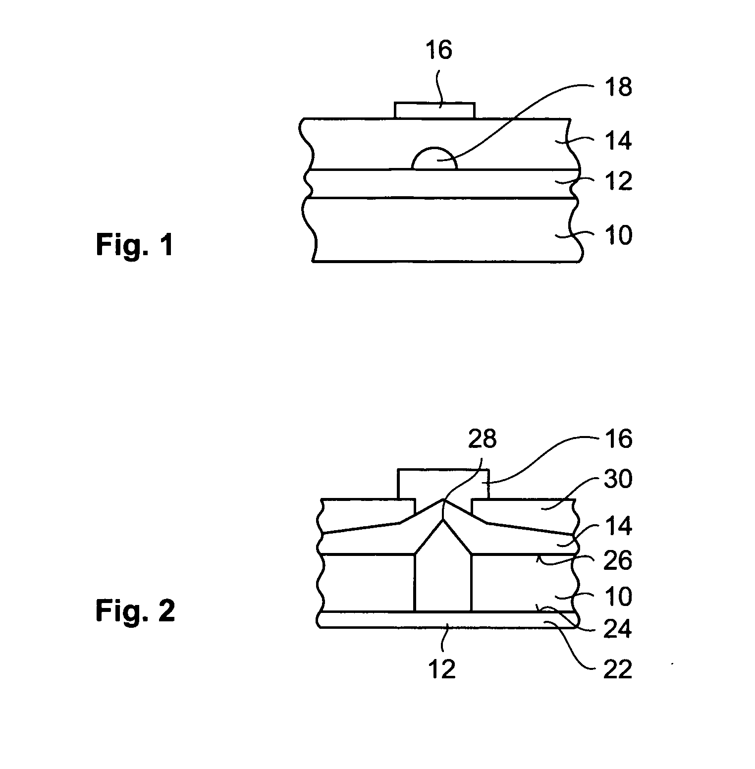
[0077] A further effect of the straining element 18 is a local enhancement of the electrical field in the insulating dielectric material. This enhancement contributes to the localization of the filament in the first embodiment, too.
[0078] The straining element 18 has the shape of a microtip or dot which is grown, deposited or etched on the first electrode 12. Its shape may be the shape of a semi-spherical hillock as shown in FIG. 1. The straining element 18 is made of a metal, such as Pt, Mo or W, a metallic oxide, such as SrRuO3 or RuO2, a silicide, such as CoSi2, a nitride, such as TaN, W2N, or a combination thereof. According to preferred embodiments the straining element 18 can be grown epitaxially or not, can be monocrystalline, polycrystalline or amorphous and can be integral with the first electrode 12. Preferentially, the straining element 18 can be integral with the first electrode 12 and made of a highly doped Si region. Advantageously, the size and shape of the straining ...
third embodiment
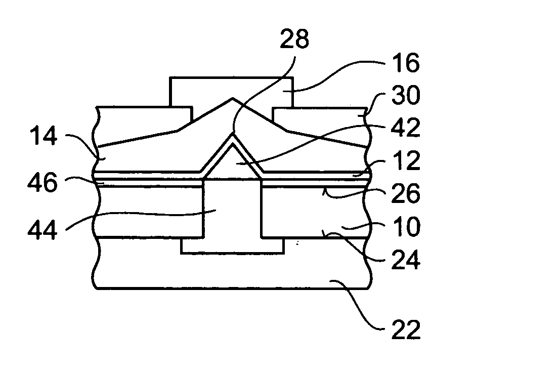
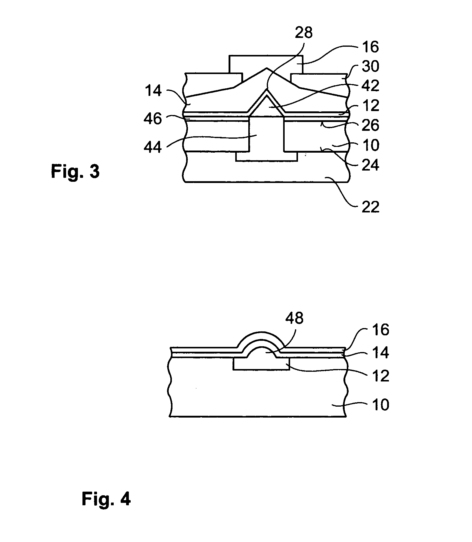
[0095] The first electrode 12 at least partially covers the surfaces of the piezo-element 42 protruding from the front surface 26 of the substrate 10. Thereby, the first electrode 12 of the third embodiment is an example for an electrode including a protrusion, or convex feature, which is caused by an element positioned between the electrode and the substrate.
[0096] The insulating dielectric material 14 is deposited on top of the first electrode 12 in a more or less uniform manner. In the vicinity of the point 28 of the first electrode 12, the insulating dielectric material 14 is sandwiched between the first electrode 12 and a second electrode 16. The insulating layer 30 covers most of the insulating dielectric material 14. The insulating layer 30 has a small hole in the vicinity of the point 28 through which the second electrode 16 is in contact with the insulating dielectric material 14. A further insulation layer 46 provides secure electrical insulation of the first electrode 12 ...
fourth embodiment
[0102]FIG. 4 is a schematic view of a vertical cross-section of a resistor according to a Again, on top of the substrate 10 the insulating dielectric material 14 is sandwiched between the first electrode 12 and the second electrode 16. The first electrode 12 comprises a protrusion 48 directed towards the second electrode 16. The protrusion 48 causes a deviation of the shape of the layer of the insulating dielectric material 14 from the flat form with parallel plane surfaces and a laterally constant thickness. Thereby, the protrusion 48 of the first electrode 12 generates a local strain field in the insulating dielectric material 14. The effect of this strain field is the same as in the above-described embodiments 1 to 3.
[0103]FIG. 5 is a schematic view of a vertical cross-section of a resistor according to a fifth preferred embodiment. An SOI wafer (SOI=silicon on isolator) comprises a bulk silicon substrate 10, a buried oxide layer (BOX-layer) 52 (isolator) and a highly doped semi...
PUM
 Abstract
Description
Claims
Application Information
 - R&D
- Intellectual Property
- Life Sciences
- Materials
- Tech Scout
- Unparalleled Data Quality
- Higher Quality Content
- 60% Fewer Hallucinations
Browse by: Latest US Patents, China's latest patents, Technical Efficacy Thesaurus, Application Domain, Technology Topic, Popular Technical Reports.
© 2025 PatSnap. All rights reserved.Legal|Privacy policy|Modern Slavery Act Transparency Statement|Sitemap|About US| Contact US: help@patsnap.com