Selective oxide trimming to improve metal T-gate transistor

a technology of metal t-gate transistor and selective oxide, which is applied in the manufacturing of semiconductor/solid-state devices, basic electric elements, electrical equipment, etc., can solve the problems of low power the need for high k material is therefore low power driven and not high performance driven, and the current siosub>2 material could reach an unacceptable gate leakage with decreasing oxide thickness, etc., to achieve the effect of reducing repetition

Active Publication Date: 2006-01-12
CHARTERED SEMICONDUCTOR MANUFACTURING
View PDF12 Cites 56 Cited by
  • Summary
  • Abstract
  • Description
  • Claims
  • Application Information

AI Technical Summary

Benefits of technology

[0021] The above and below advantages and features are of representative embodiments only, and are not exhaustive and / or exclusive. They are presented only to assist in understanding the invention. It should be understood that they are not representative of all the inventions defined by the claims, to be considered limitations on the invention as defined by the claims, or limitations on equivalents to the claims. For instance, some of these advantages may be mutually contradictory, in that they cannot be simultaneously present in a single embodiment. Similarly, some advantages are applicable to one aspect of the invention, and inapplicable to others. Furthermore, certain aspects of the claimed invention have not been discussed herein. However, no inference should be drawn regarding those discussed herein relative to those not discussed herein other than for purposes of space and reducing repetition. Thus, this summary of features and advantages should not be considered dispositive in determining equivalence. Additional features and advantages of the invention will become apparent in the following description, from the drawings, and from the claims.

Problems solved by technology

The advancement in transistor technology has led to numerous emerging issues.
ITRS 2001 has shown that by 2005, the current SiO2 material could have reached an unacceptable gate leakage with decreasing oxide thickness.
The need for High K material is therefore low power driven and not high performance driven.
In addition, lithography is also another challenging area whereby gate length is scaled aggressively too.
Another scaling issue would be the polysilicon gate / SiO2 system.
These would make current silicon dioxide material seems almost impossible for future transistor technology.

Method used


Image

  • Selective oxide trimming to improve metal T-gate transistor
  • Selective oxide trimming to improve metal T-gate transistor
  • Selective oxide trimming to improve metal T-gate transistor

Examples


first example embodiment

II. First Example Embodiment

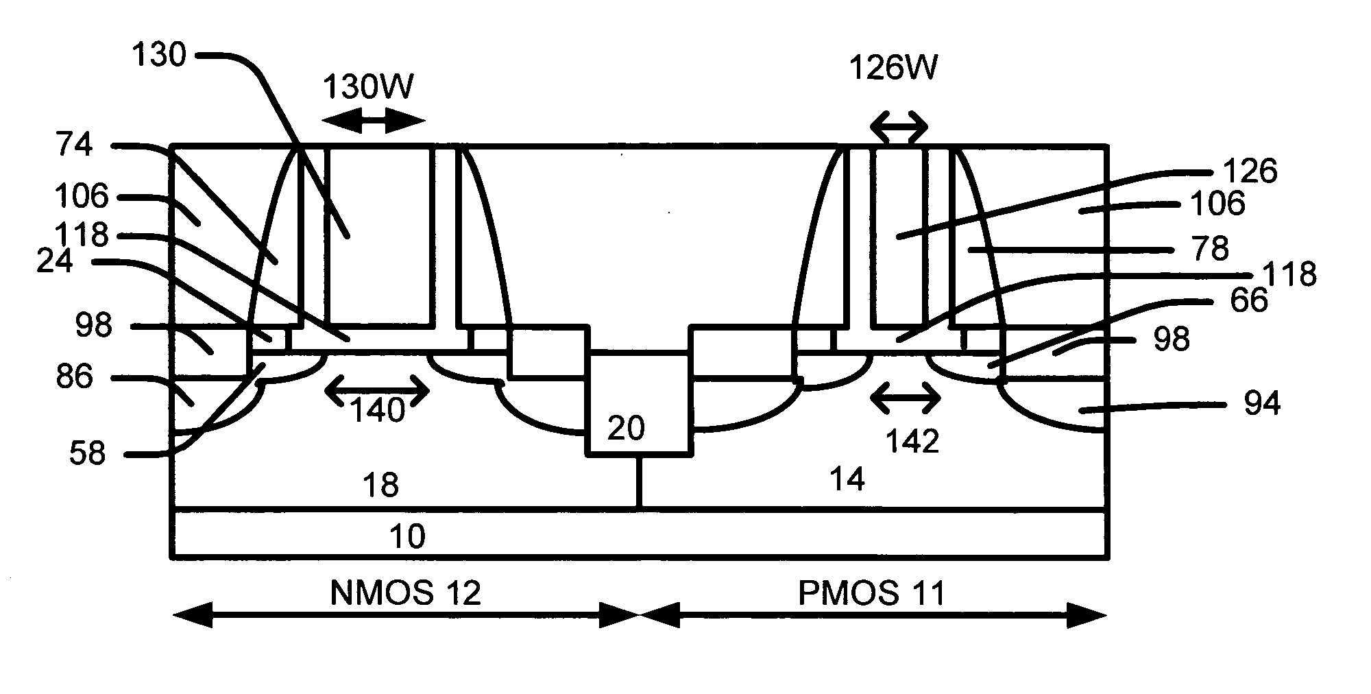
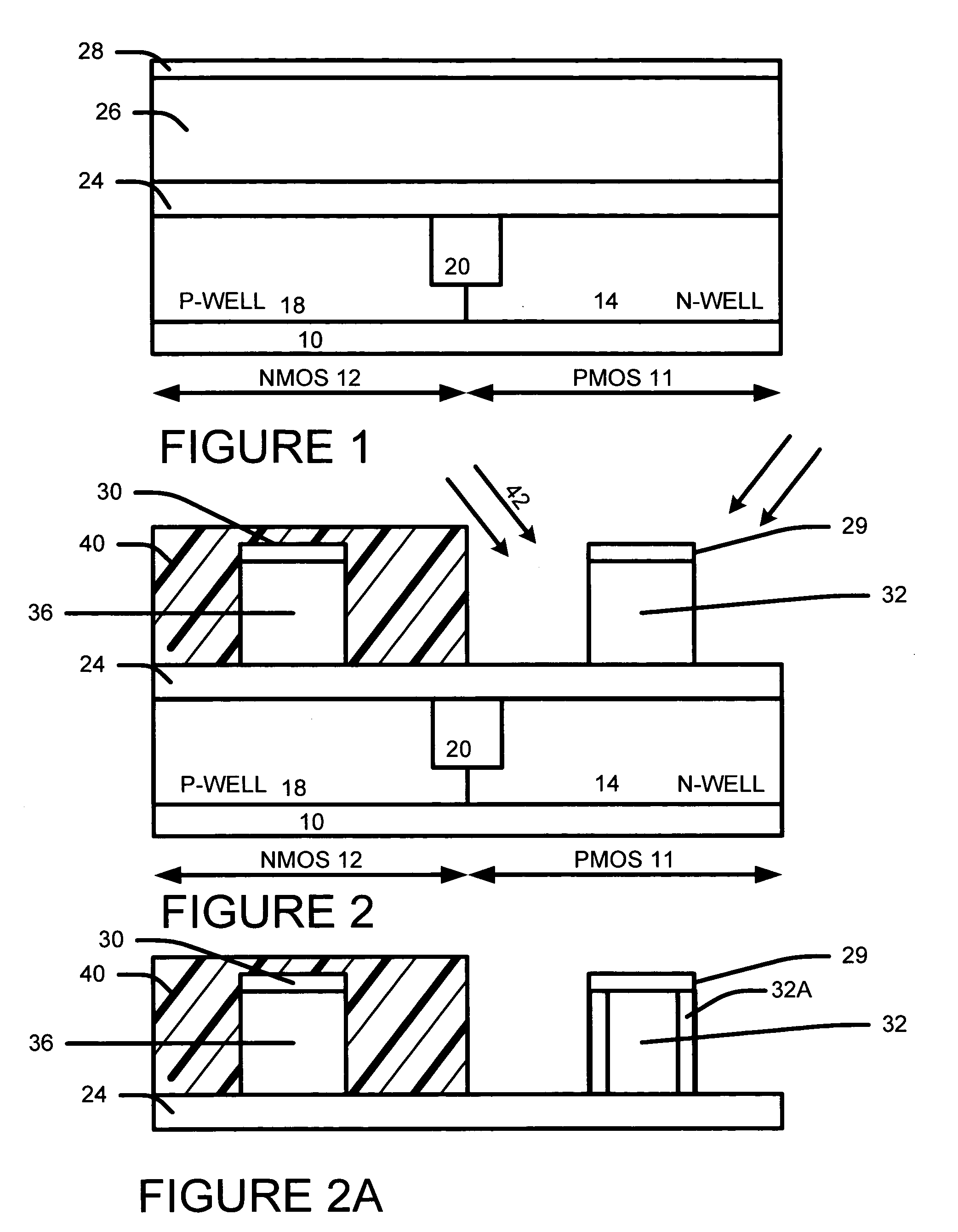
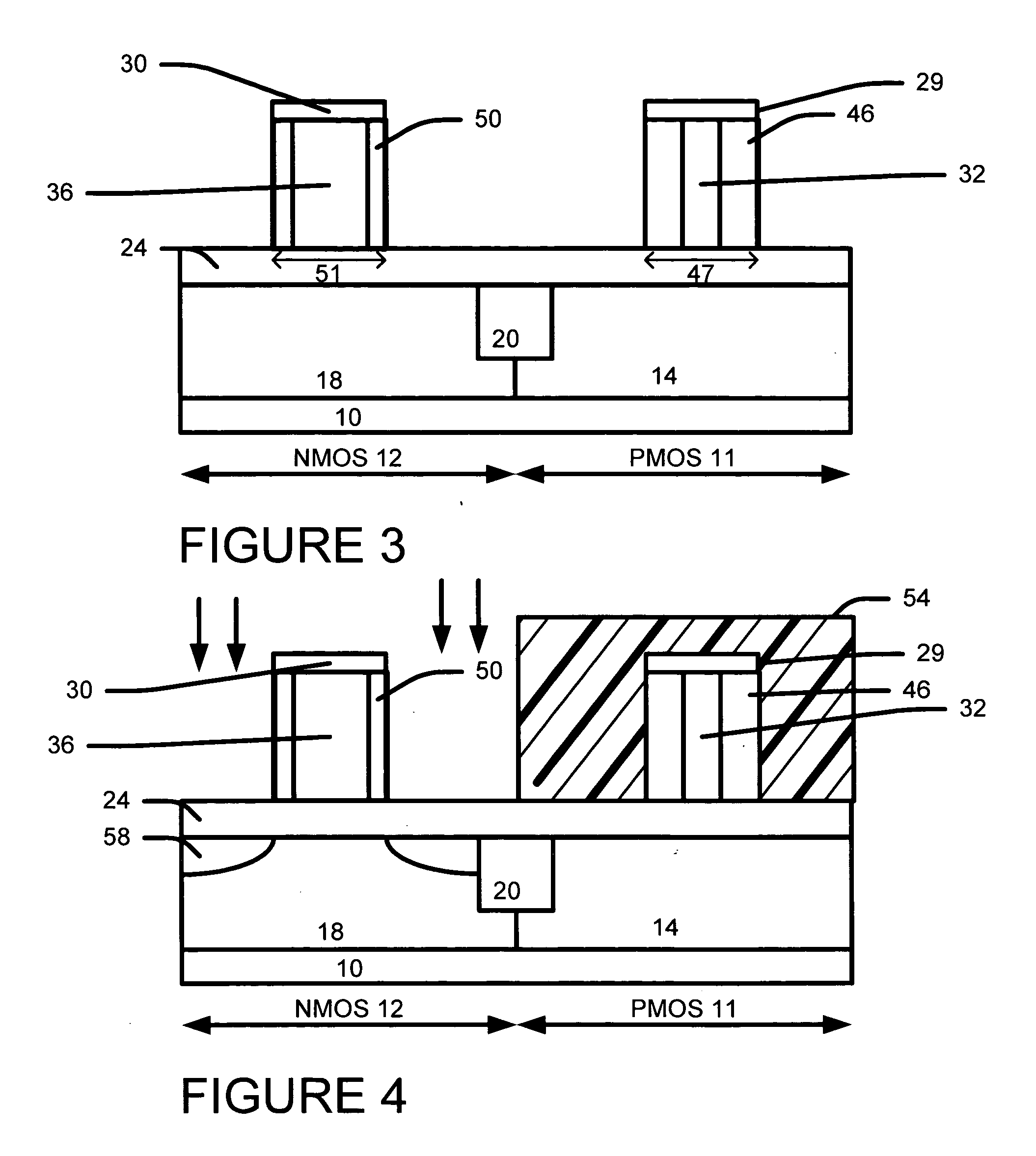
[0034] Referring to FIG. 1, we form a n-well 14 in PMOS area 11 and a p-well 18 in a NMOS area 12 in a substrate 10. The substrate can be silicon wafer and other substrate using in semiconductor manufacturing.

[0035] Next, we form isolation regions 20 in the substrate 10. The isolation regions are preferably shallow trench isolation (STI) regions.

[0036] We then form a bottom pad dielectric layer 24, a silicon containing layer (e.g., polysilicon layer) 26 and a hard mask layer 28 over the substrate. The polysilicon layer preferably contains polysilicon. The polysilicon layer can be comprised of polysilicon, amorphous silicon or SiGe.

[0037] The bottom pad dielectric layer 24 is preferably comprised of oxide and has a thickness between 50 and 400 Å.

[0038] The silicon containing layer ( e.g., polysilicon layer) 26 preferably has a thickness between 1000 and 2000 Å.

[0039] The hard mask layer 28 is preferably comprised of nitride. The hard mask layer is use...

second example embodiment

III. Dual Work Function Metal Gate

[0105] FIGS. 1 to 14 and FIGS. 18 to 23 show an embodiment with an optional dual work function metal gate process flow. The embodiment forms two types of gate comprised of different materials. For example, FIG. 23 shows a NMOS gate 240 that can be made of a different metal than PMOS gate 212.

[0106] The process flow is basically the same as the first embodiment as shown in FIGS. 1 to 14.

[0107] Referring to FIG. 18, we form a PMOS poly etch mask 200 having an PMOS poly opening over the PMOS area 11. The etch mask 200 is preferably comprised of photoresist.

[0108] As shown in FIG. 18, we remove the PMOS sacrificial gate 32 and portions of the bottom pad dielectric layer 24 to form a PMOS gate openings 202 that exposes portions of the bottom pad dielectric layer 24.

[0109] Then we remove the exposed portions of the bottom pad dielectric layer 24 in the PMOS gate openings 202. As noted above in the description of the first example embodiment, the under...


PUM


Abstract

A process to form a FET using a replacement gate. An example feature is that the PMOS sacrificial gate is made narrower than the NMOS sacrificial gate. The PMOS gate is implanted preferably with Ge to increase the amount of poly sacrificial gate that is oxidized to form PMOS spacers. The spacers are used as masks for the LDD Implant. The space between the PLLD regions is preferably larger that the space between the NLDD regions because of the wider PMOS spacers. The PLDD tends to diffuse readily more than NLDD due to the dopant being small and light (i.e. Boron). The wider spacer between the PMOS regions improves device performance by improving the short channel effects for PMOS. In addition, the oxidization of the sacrificial gates allows trimming of sacrificial gates thus extending the limitation of lithography. Another feature of an embodiment is that a portion of the initial pad oxide is removed, thus reducing the amount of undercut created during the channel oxide strip for the dummy gate process. This would improve on the gate overlap capacitance for a T-gate transistor. In a second embodiment, two metal gates with different work functions are formed.

Description

BACKGROUND OF INVENTION [0001] 1) Field of the Invention [0002] This invention relates generally to fabrication of semiconductor devices and more particularly to the fabrication of a FET with a metal gate. [0003] 2) Description of the Prior Art [0004] The advancement in transistor technology has led to numerous emerging issues. Gate oxide is one of the most aggressively scaled parameter to maintain the Moore's Law. ITRS 2001 has shown that by 2005, the current SiO2 material could have reached an unacceptable gate leakage with decreasing oxide thickness. Hence, new material is needed to replace silicon dioxide by then. [0005] Currently, the semiconductor workers are hot on the heels in search of new materials, the more promising ones at this point in time is High K materials (HfO and ZrO, etc). High K materials would provide a lower EOT for a given thickness which would reduce the stringent requirement compared to silicon dioxide in terms of thickness requirement. The need for High K...

Claims


Application Information

Patent Timeline
Patent Type & Authority Applications(United States)
IPC IPC(8): H01L21/336H01L21/8238
CPCH01L21/26586H01L21/28079H01L21/28123H01L21/823842H01L29/66545H01L21/823857H01L29/495H01L29/6653H01L21/82385
Inventor PHUA, TIMOTHY WEE HONGTEE, KHENG CHOKHSIA, LIANG CHOO
Owner CHARTERED SEMICONDUCTOR MANUFACTURING
Why Eureka
Try Eureka