Electron emitter

a technology of electron emitter and emitter, which is applied in the field of electron emitter, can solve the problems of increasing production costs of not only the electron emitter itself but also the device to which the electron emitter is applied, complicated production processes, and high production costs of the electron emitter, so as to achieve the effect of increasing the number of electric field concentrated portions, increasing the amount of emitted electrons, and easy obtaining high electric field concentration

Inactive Publication Date: 2006-01-19
NGK INSULATORS LTD
View PDF4 Cites 29 Cited by
  • Summary
  • Abstract
  • Description
  • Claims
  • Application Information

AI Technical Summary

Benefits of technology

[0071] As explained above, an electron emitter according to the present invention makes it possible to easily obtain a high electric field concentration and moreover to increase the number of the electric field concentrated portions. Thereby it becomes possible to provide an electron emitter capable of increasing the amount of emitted electrons.

Problems solved by technology

Hence, in order to form such a minuscule conductive electrode, fine processing by etching, forming or the like has been required and that has caused production processes to be complicated.
Further, a certain degree of high voltage has been required as the drive voltage in order to emit a prescribed amount of electrons from the edge of the conductive electrode into a vacuum of a prescribed vacuum level, and thus, as a drive element such as an IC, an expensive one withstanding the high voltage drive to drive the electron emitter has been required.
As stated above, the problem of the electron emitter using a conductive electrode as an emitter has been that the production costs of not only the electron emitter itself but also the device to which the electron emitter is applied increase.

Method used


Image

  • Electron emitter
  • Electron emitter
  • Electron emitter

Examples


example 1

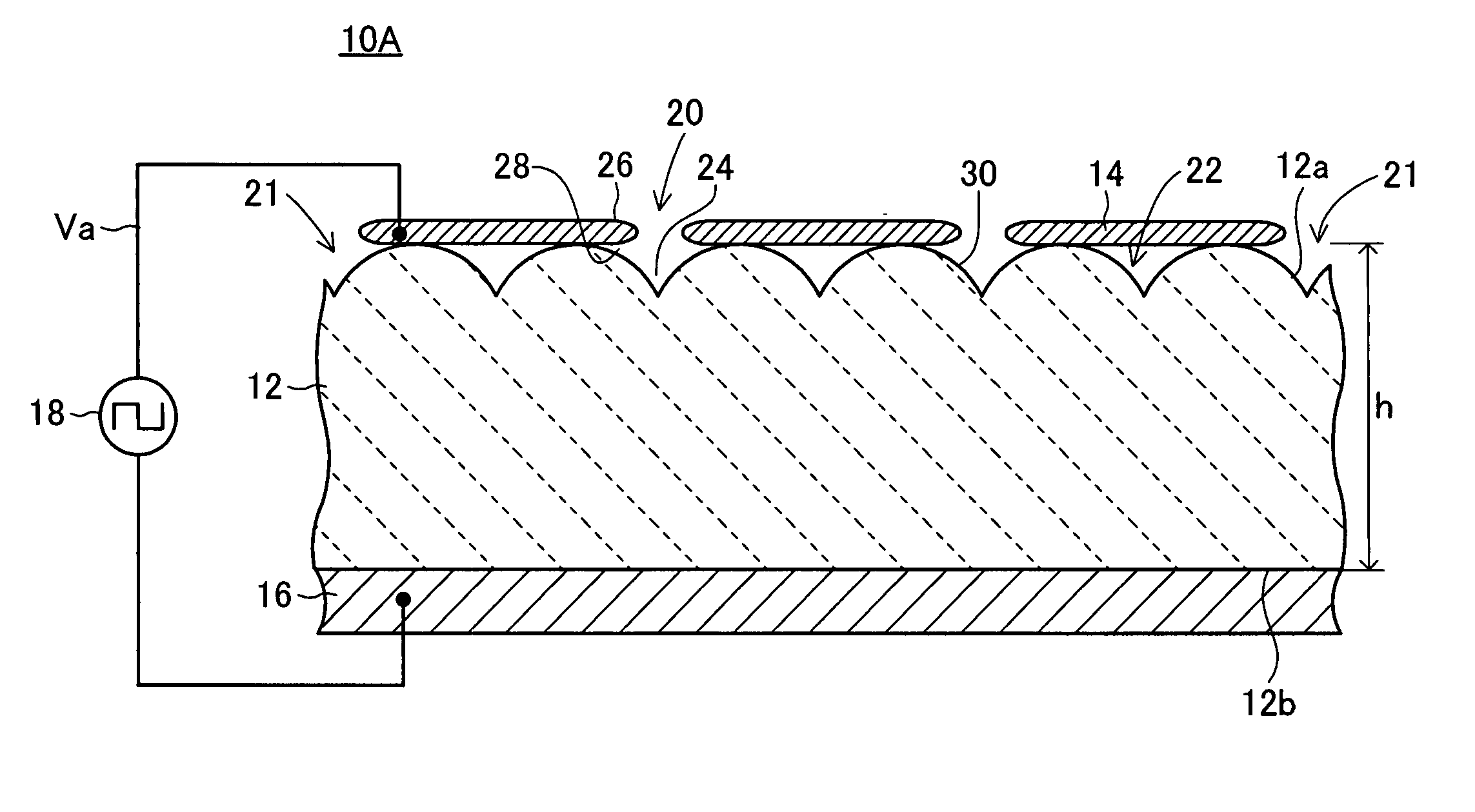
[0125] Here, a preferable example of an electron emitter according to the present invention is explained on the basis of FIG. 9. In the electron emitter 110A of the first example, the emitter 12 includes many first dielectric particles 12e and second dielectric particles 12f. The first dielectric particles 12e are relatively coarse particles the size of which is 1 μm or larger and the second dielectric particles 12f are made of the same material as the first dielectric particles 12e and are fine particles having sizes of submicron level. Then the second dielectric particles 12f are disposed so as to fill the spaces surrounded by the many first dielectric particles 12e.

[0126] Here, since the upper surface 12a of the emitter 12 serves to emit electrons by applying a prescribed electric field, if there are particles of too small size s, defects such as crystal grain boundaries increase and the relative dielectric constant lowers and consequently the applied field intensity undesirably...

example 2

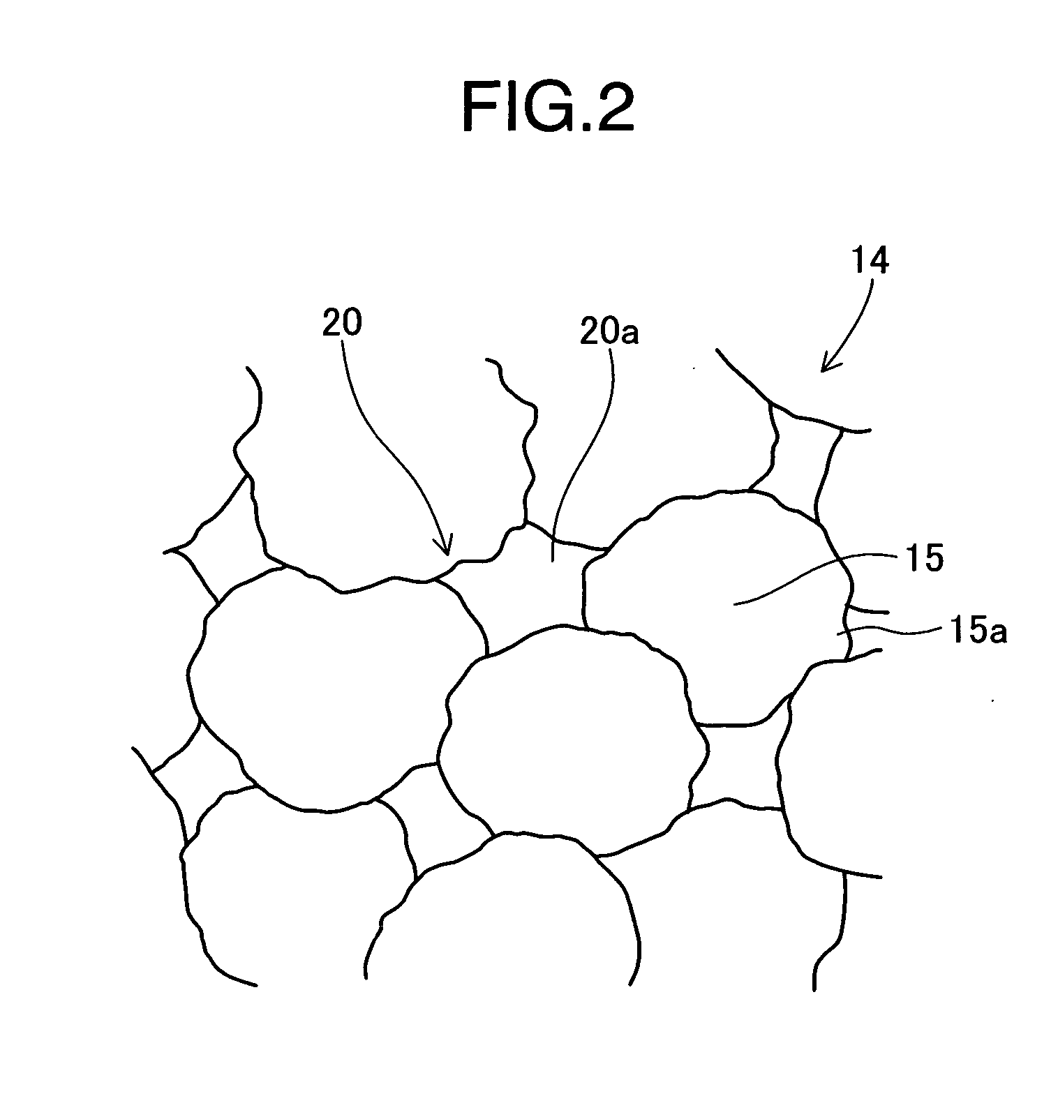
[0130] Further, an electron emitter 210A according to the second preferable example is explained referring to FIG. 10. In the electron emitter 210A according to the second example, the emitter 12 has a double-layered structure including the first layer 12c composing the uppermost layer of the emitter 12 and the second layer 12d located under the first layer 12c and formed on the lower electrode 16. Then the upper surface of the first layer 12c composes the upper surface 12a of the emitter 12. Here, the first layer 12c includes a large number of the first dielectric particles 12e.

[0131] Since, as stated above, the upper surface of the first layer 12c composes the upper surface 12a of the emitter 12 that has the function of emitting electrons when a prescribed electric field is applied, in particular if the size of the first dielectric particles 12e composing the first layer 12c is too small, defects such as crystal grain boundaries and others increase, resulting in the lowering of t...


PUM


Abstract

A dielectric device of higher performance is provided. An electron emitter, to which the dielectric device is applied is provided with: an emitter including a dielectric; and an upper electrode and a lower electrode to which drive voltage is applied in order to emit electrons. The emitter is formed by the aerosol deposition method or the sol impregnation method.

Description

BACKGROUND OF THE INVENTION [0001] 1. Field of the Invention [0002] The present invention relates to an electron emitter that can be applied as an electron beam source in various devices, using electron beams, such as a display including a field emission display (FED), an electron beam irradiation device, a light source, electronic parts manufacturing apparatus, and an electronic circuit part. [0003] 2. Description of the Related Art [0004] Such an electron emitter is, as is well known, operated in a vacuum of a prescribed vacuum level, and configured so that electrons are emitted from electron emission portions (hereunder referred to as “emitters”) by applying a prescribed electric field to the emitters. When such an electron emitter is applied to an FED, plural electron emitters are arranged two-dimensionally and plural phosphors are disposed at prescribed intervals to the electron emitters so that each of the phosphors corresponds to each of the electron emitters. Then, an electr...

Claims


Application Information

Patent Timeline
Patent Type & Authority Applications(United States)
IPC IPC(8): H01J9/02
CPCB82Y10/00H01J1/312H01J2329/00H01J29/481H01J9/025
Inventor NANATAKI, TSUTOMUYAMAGUCHI, HIROFUMITANAKA, RITSU
Owner NGK INSULATORS LTD
Why Eureka
Try Eureka