
Microstructured infrared sensor and method for its manufacture

Inactive Publication Date: 2006-01-26
ROBERT BOSCH GMBH
View PDF13 Cites 52 Cited by
  • Summary
  • Abstract
  • Description
  • Claims
  • Application Information

AI Technical Summary

Benefits of technology

[0008] Due to the increased sensitivity, the number of thermopiles, i.e., printed conductors, may be reduced. According to the present invention, the lateral dimensions of the diaphragm and of the absorber layer may also be reduced.
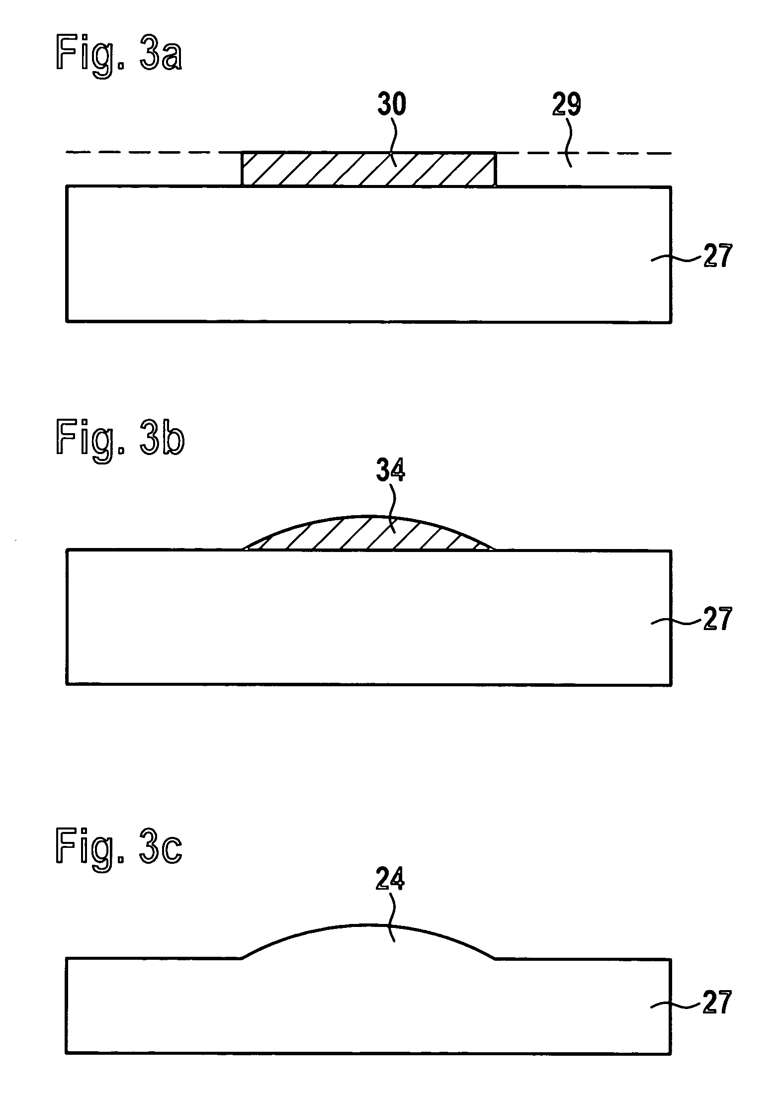
[0014] Compared to photolithography or special lithography, spin-on deposition and a prebake step of the first layer, spin-on deposition and prebake step of the second layer, edge lacquer removal, exposure, subsequent developing, and the required lacquer height control are no longer needed in the case of direct dispensing. The 10-minute dispensing step, for example, is also considerably shorter than the 45-minute swelling process required in special lithography, and the 2-hour drying, for example, according to the present invention is somewhat shorter than the 3-hour drying, for example, required for special lithography. The time for the overall process may thus be reduced by 60%, for example, and handling time by workers may be reduced by as much as over 80%.
[0015] Furthermore, smaller amounts of material are used in direct dispensing, because no excess material remains at the end of the process, in contrast to a process in which layers are applied and subsequently structured. Also, no developer, no solvent for swelling, and no photoresist are required, so that a considerable additional savings in materials may also be achieved.

Problems solved by technology

Due to the large surface area needed and the complex design of the large thermopile structures, high costs are incurred in manufacturing the infrared sensor and the sensor module made up of the sensor, the package, and the cover.

Method used


Image

  • Microstructured infrared sensor and method for its manufacture
  • Microstructured infrared sensor and method for its manufacture
  • Microstructured infrared sensor and method for its manufacture

Examples


Embodiment Construction

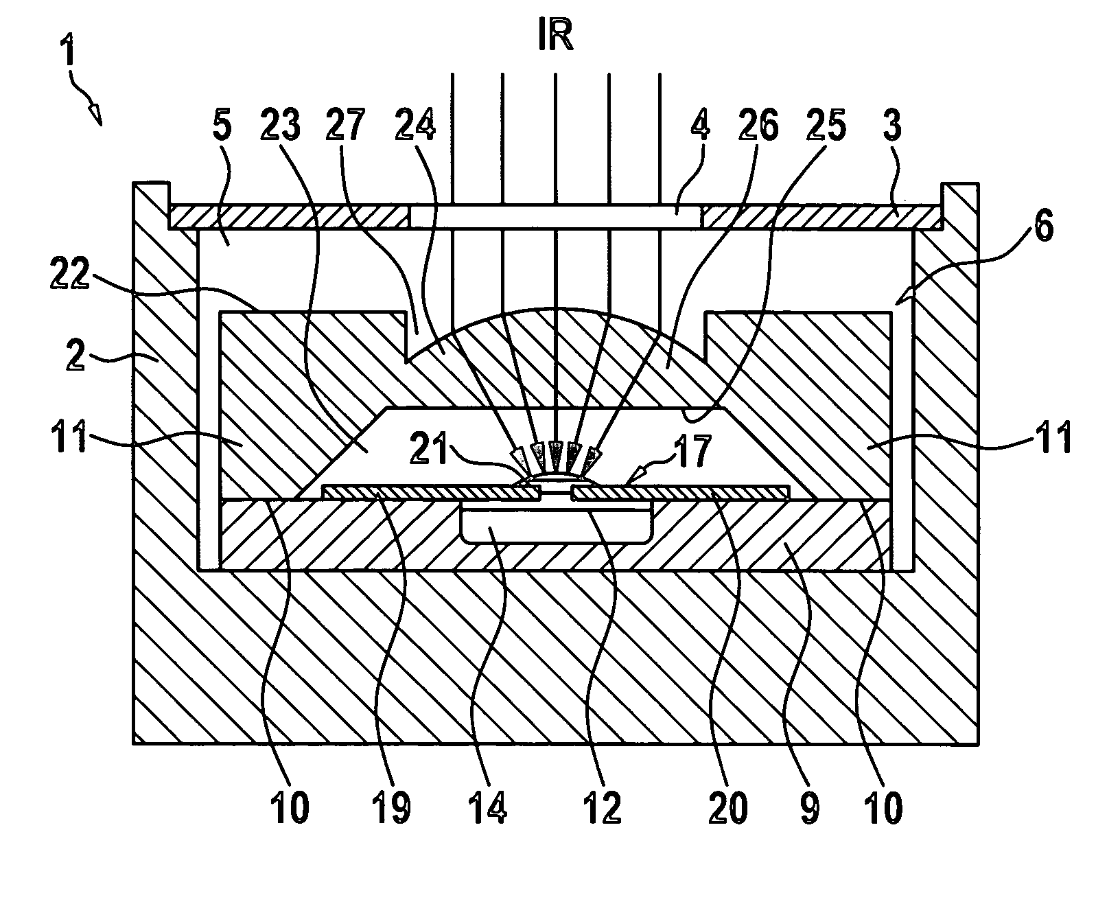
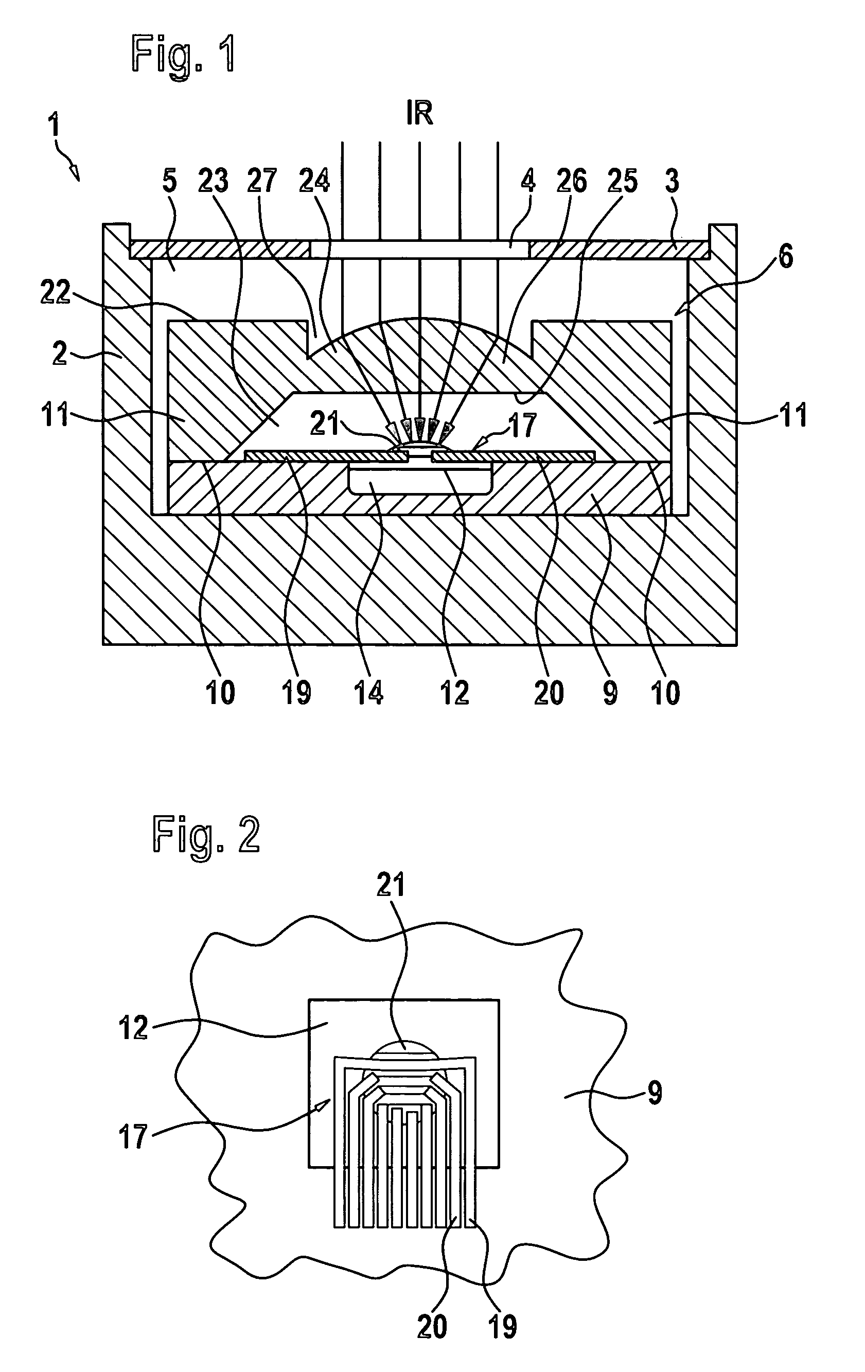
[0023] As shown in FIG. 1, infrared sensor module 1 has a package 2 made of a molded compound or ceramic, for example, and a cover 3 attached to package 2 having a screen aperture 4. An infrared sensor 6 is placed in package inner space 5 formed between package 2 and cover 3. The infrared sensor 6 has a sensor chip 9 glued onto the bottom of package 2 and a cap chip 11 attached to sensor chip 9 by seal glass bond 10. Situated on the sensor chip 9, above a cavity 14 of the sensor chip 9, is a diaphragm 12. Diaphragm 12 and cavity 14 may be formed, for example, by forming or depositing an SiO2 or Si3N4 layer on the substrate of sensor chip 9, structuring etched openings, etching cavity 14 underneath the layer, and subsequently sealing the etched openings.

[0024] Alternative to the embodiment shown in FIG. 1, a cavity 14 may be formed from the bottom of sensor chip 9 via KOH etching, for example, and the etching process may be stopped when a sufficiently thin diaphragm 12 has formed on...


PUM


Abstract

A microstructured infrared sensor includes: a sensor chip having a diaphragm; a cavity formed underneath the diaphragm; a thermopile structure formed on the diaphragm and having bonded printed conductors; an absorber layer formed on the thermopile structure for absorbing infrared radiation; and a cap chip attached to the sensor chip. A sensor space is formed between the cap chip and the sensor chip, and the sensor space accommodates the thermopile structure. The infrared sensor also includes a convex lens area for focusing incident infrared radiation onto the absorber layer. The lens area may be formed on the top of the cap chip or on a lens chip attached to the cap chip. The lens area may be formed by drying a dispensed lacquer droplet, or by a softened, structured lacquer cylinder, or by subsequent etching of the dried lacquer droplet and the surrounding substrate material.

Description

FIELD OF THE INVENTION [0001] The present invention relates to a microstructured infrared sensor and a method for its manufacture. BACKGROUND INFORMATION [0002] Microstructured infrared sensors may be used, e.g., in gas detectors, in which IR (infrared) radiation emitted by a radiation source, an incandescent bulb operated in the low-current range, or an IR LED, for example, is transmitted over a measuring path and subsequently received by the infrared sensor, and the concentration of the gases to be detected in the measuring path is estimated from the absorption of the infrared radiation in specific wavelength ranges. Gas sensors of this type may be used, e.g., in automobiles, for example, for detecting a leak in an air conditioning unit operated using CO2, or for checking the air quality of the ambient air. [0003] In general, microstructured infrared sensors have a sensor chip as a substrate in which a diaphragm, underetched by a cavity, is formed. At least one thermopile structur...

Claims


Application Information

Patent Timeline
IPC IPC(8): G01J5/00
CPCG01J1/04H01L31/0232G01J5/02G01J5/0215G01J5/024G01J5/04G01J5/045G01J5/046G01J5/08G01J5/0806G01J5/0853G01J5/0881G01J5/12G01N21/3504H01L27/14618H01L27/14625H01L31/0203G01J1/0411H01L2924/0002H01L2924/00
Inventor KUMMER, NILSMUELLER-FIEDLER, ROLANDFINKBEINER, STEFANMUELLER, ANDREMUENZEL, HORSTMAURER, DIETERHIEMER, STEFANPERTHOLD, JURGEN
Owner ROBERT BOSCH GMBH
Learn More