

Double-layer chiral micro-nano structure and preparation method thereof
A micro-nano structure and chirality technology, applied in optics, instruments, optical components, etc., can solve the problem that the molecular self-assembly laser direct writing method cannot prepare nano-scale structural features, and it is difficult to prepare artificial chiral surface plasmon structures. It is difficult to solve the problem of high difficulty, and achieves the effect of good application prospect, flexible and convenient application, and simplified preparation process steps.
- Summary
- Abstract
- Description
- Claims
- Application Information
AI Technical Summary
Problems solved by technology
Method used
Image

Examples
Embodiment 1
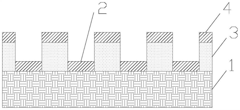
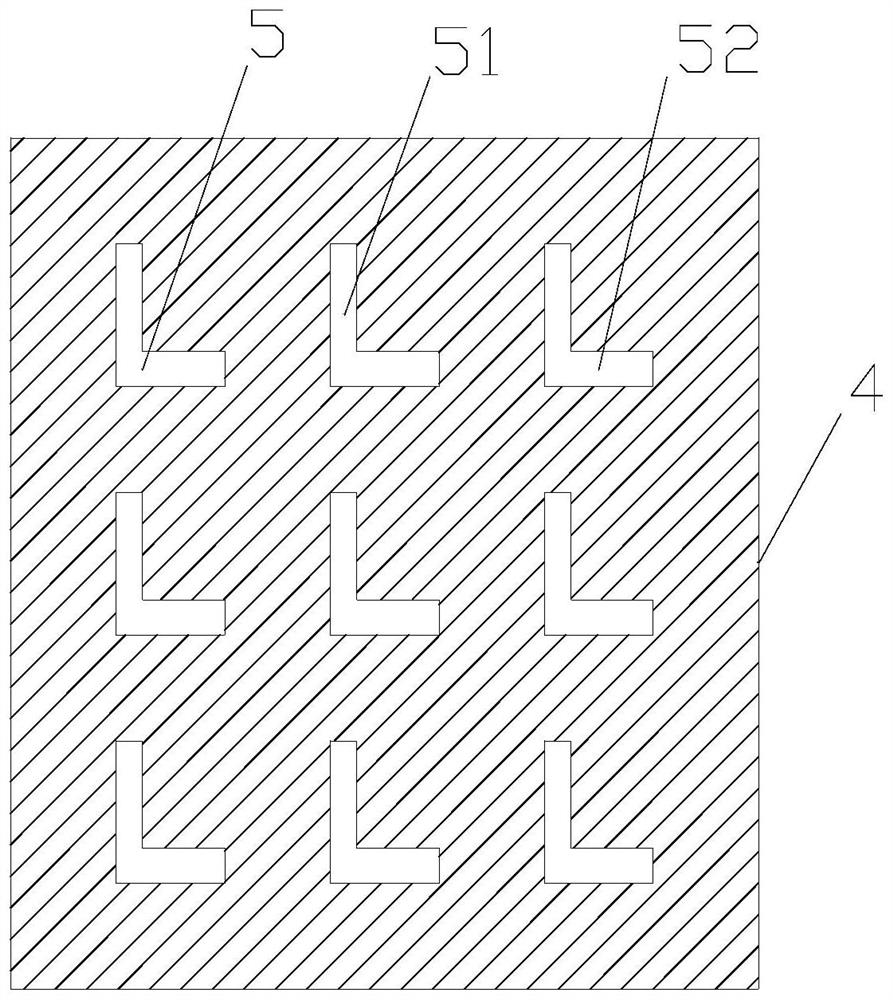
[0032] The invention provides a double-layer chiral micro-nano structure, such as figure 1 As shown, it includes a substrate, a second noble metal layer, a transparent medium layer, and a first noble metal layer. The transparent medium layer is placed on the substrate, and the material of the substrate is conductive glass, which is convenient for conducting electricity during electron beam etching, so that the charges can be conducted without irregularities in the etched samples caused by charge accumulation. The material of the transparent medium layer is PMMA. The first noble metal layer is placed on the transparent medium layer, and the material of the first noble metal layer is silver or gold. Such as figure 2 As shown, there are L-shaped holes penetrating through the first noble metal layer and the transparent medium layer, that is, the L-shaped holes penetrate the first noble metal layer and the transparent medium layer, and reach the surface of the substrate. The L-...
Embodiment 2
[0035] On the basis of Example 1, the thickness of the nanorods is less than the thickness of the transparent medium layer, so that there is a certain distance between the lower surface of the first noble metal layer and the upper surface of the nanorods, and the distance between the first noble metal layer and the nanorods is applied. The coupling between them produces circular dichroism in the transmitted light. Preferably, the distance between the lower surface of the first noble metal layer and the upper surface of the nanorods is greater than 10 nanometers and less than 240 nanometers, so that the coupling between the thin film and the nanorods can be achieved.
Embodiment 3
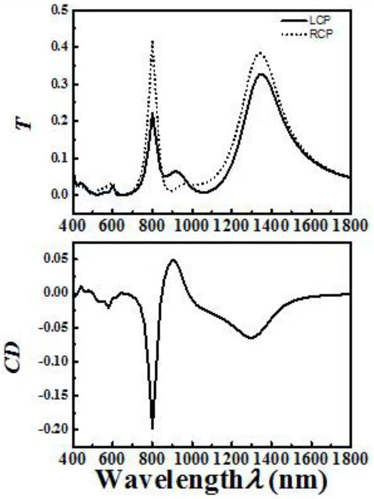
[0037] On the basis of Example 2, a double-layer chiral micro-nanostructure with specific morphology parameters was designed, and the transmission spectrum, circular dichroism spectrum and The charge distribution at the resonance mode is used to illustrate and illustrate the core principles of the present invention.
[0038]The material of the first noble metal layer and the second noble metal layer is silver. The transparent medium layer is PMMA. The material of the substrate is conductive glass with a refractive index of 1.45. The thickness of the first noble metal layer is 60 nanometers. The first arm of the hole has a length of 260 nm and a width of 80 nm. The second arm of the hole has a length of 320 nm and a width of 80 nm. The periods of the L-shaped holes are 600 nm and 600 nm. The thickness of the transparent medium layer is 60 nanometers. The thickness of the nanorods is the same as that of the first noble metal layer. The length and width of the nanorods are...
PUM
| Property | Measurement | Unit |
|---|---|---|
| Thickness | aaaaa | aaaaa |
| Thickness | aaaaa | aaaaa |
Abstract
Description
Claims
Application Information