

Semiconductor device
a semiconductor and device technology, applied in the direction of semiconductor devices, semiconductor/solid-state device details, electrical apparatus, etc., can solve the problems of off-chip sso noise, simultaneous switching of a large number of switching elements, and increase the cost of the device, so as to reduce the noise on-chip
- Summary
- Abstract
- Description
- Claims
- Application Information
AI Technical Summary
Benefits of technology
Problems solved by technology
Method used
Image

Examples
embodiment 1
[0041] Before embodiments are described, how On-Chip SSO noise occurs is described below.
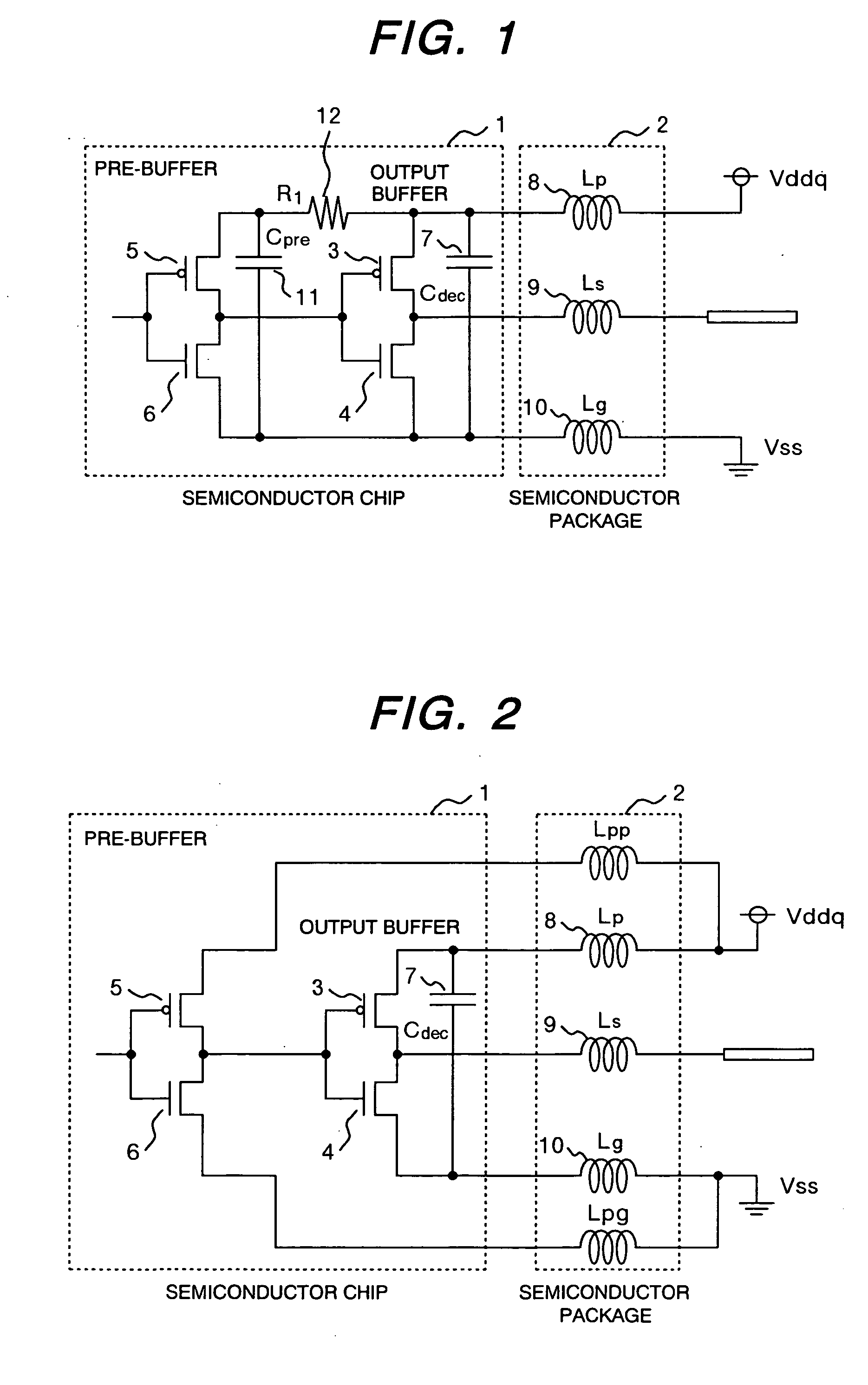
[0042] A schematic diagram of internal circuits of a semiconductor device for transmitting electrical signals to the outside of a chip by switching a CMOS section of an output buffer is shown in FIG. 7. The semiconductor device is constituted by the semiconductor chip shown as 1 in FIG. 7, and the semiconductor package of 2 in FIG. 7 that seals the semiconductor chip, and a power supply voltage “Vddq” based on a grounding potential “Vss” is fed from the system to the semiconductor device. In FIG. 7, only two stages, i.e., an output buffer formed as a CMOS section having the PMOS and NMOS denoted by reference numerals 3 and 4, respectively, and a pre-buffer formed as a CMOS section having the PMOS and NMOS denoted by reference numerals 5 and 6, respectively, are depicted for simplification of the figure. Actually, however, plural output buffers and pre-buffers are present. For the sake of conven...
embodiment 2
[0056] One method of suppressing On-Chip SSO noise is, as described in the section on how the noise occurs, by changing a noise-inducing current to an overdamped state. Overdamping is accomplished by assigning the electrical parameters that satisfy QRpg≥2LpkgCdec(Expression 1)
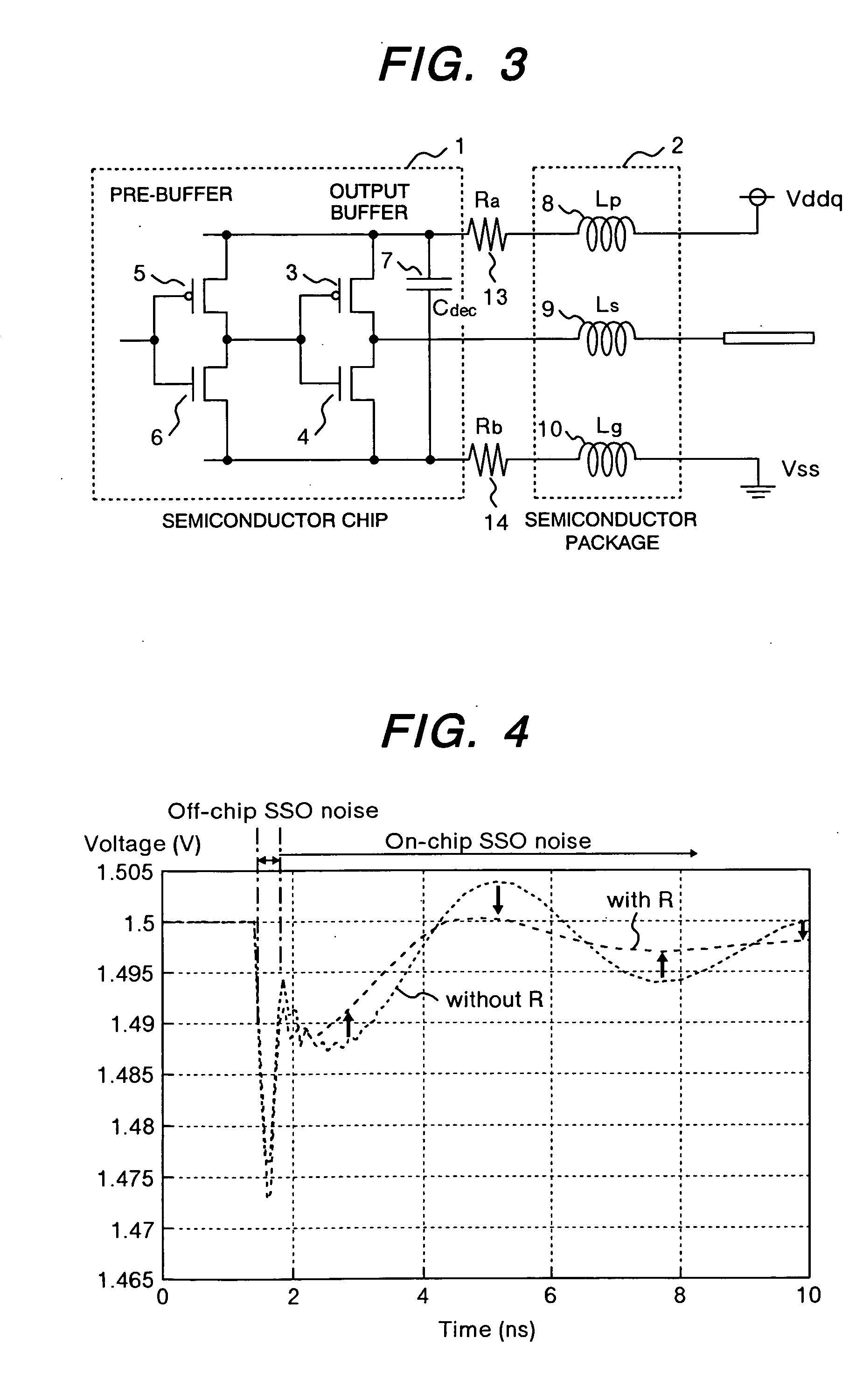
[0057] A circuit composition with resistors inserted between a semiconductor chip and a semiconductor package in order to satisfy the condition of expression 1 is Embodiment 2, a simplified equivalent circuit of which is shown in FIG. 3. Embodiment 2 is characterized in that depending on electrical characteristics of the semiconductor chip and the semiconductor package, an appropriate resistance value to be applied to a section at which the chip and the package are connected can be selected. To obtain a noise suppression effect, the terminal-to-terminal voltage waveform of an output buffer that suffers damped oscillation needs to be damped to at least ½ of a voltage waveform of an input signal to the output ...
embodiment 3
[0060] A circuit composition with a resistor inserted in series into an on-chip capacitor in order to satisfy the condition of expression 1 is Embodiment 3, a simplified equivalent circuit of which is shown in FIG. 5. Embodiment 3 is characterized in that it suppresses noise without reducing a resistance value of a power supply potential or increasing a grounding potential.
[0061] In FIG. 5, a resistor 15 is inserted into such general circuit as shown in FIG. 7. The resistor 15 is to have a resistance value that satisfies expression 1. An effect by the insertion of the resistor is shown in FIG. 6. In a semiconductor device having plural output buffers, as with the semiconductor device of FIG. 4, when a “High” output to a signal line in one of the plural output buffers is maintained at a fixed level and output levels of all other output buffers change from “High” to “Low”, voltage waveforms of the signal line fixed at the “High” output level look as in FIG. 6 which shows simulated ob...
PUM
 Abstract
Description
Claims
Application Information