
Mask pattern correction device, method of correcting mask pattern, light exposure correction device, and method of correcting light exposure

Inactive Publication Date: 2006-01-26
FUJITSU SEMICON LTD
View PDF7 Cites 0 Cited by
  • Summary
  • Abstract
  • Description
  • Claims
  • Application Information

AI Technical Summary

Benefits of technology

[0018] According to the present invention, it is made possible to estimate and correct flare with an extremely high accuracy, over the entire portion not only of a single shot region, but also of a single chip region, to thereby realize a lithographic process causative of only an extremely small dimensional variation in line width, and further to thereby realize highly-reliable semiconductor devices.

Problems solved by technology

In this sort of projection exposure apparatus, light ascribable to some optical routes not intended on the design basis, tends to generate due to reflection and scattering on the surface or inside of lenses in the lighting optical system, photomask, projection lens and so forth, or due to non-uniformity in refractive index of lens materials.
The above-described conventional technique could certainly estimate the local flares, which have never been even noticed as a problem to a reasonable degree, with a high accuracy, but it has been found that the method was suffering from difference in the correction accuracy locally in a single shot region, and could not be said as having reached a satisfactory accuracy yet.

Method used


Image

  • Mask pattern correction device, method of correcting mask pattern, light exposure correction device, and method of correcting light exposure
  • Mask pattern correction device, method of correcting mask pattern, light exposure correction device, and method of correcting light exposure
  • Mask pattern correction device, method of correcting mask pattern, light exposure correction device, and method of correcting light exposure

Examples


first embodiment

[0054] Mask pattern data correction adapted to middle(short)-range flare will be explained in this embodiment.

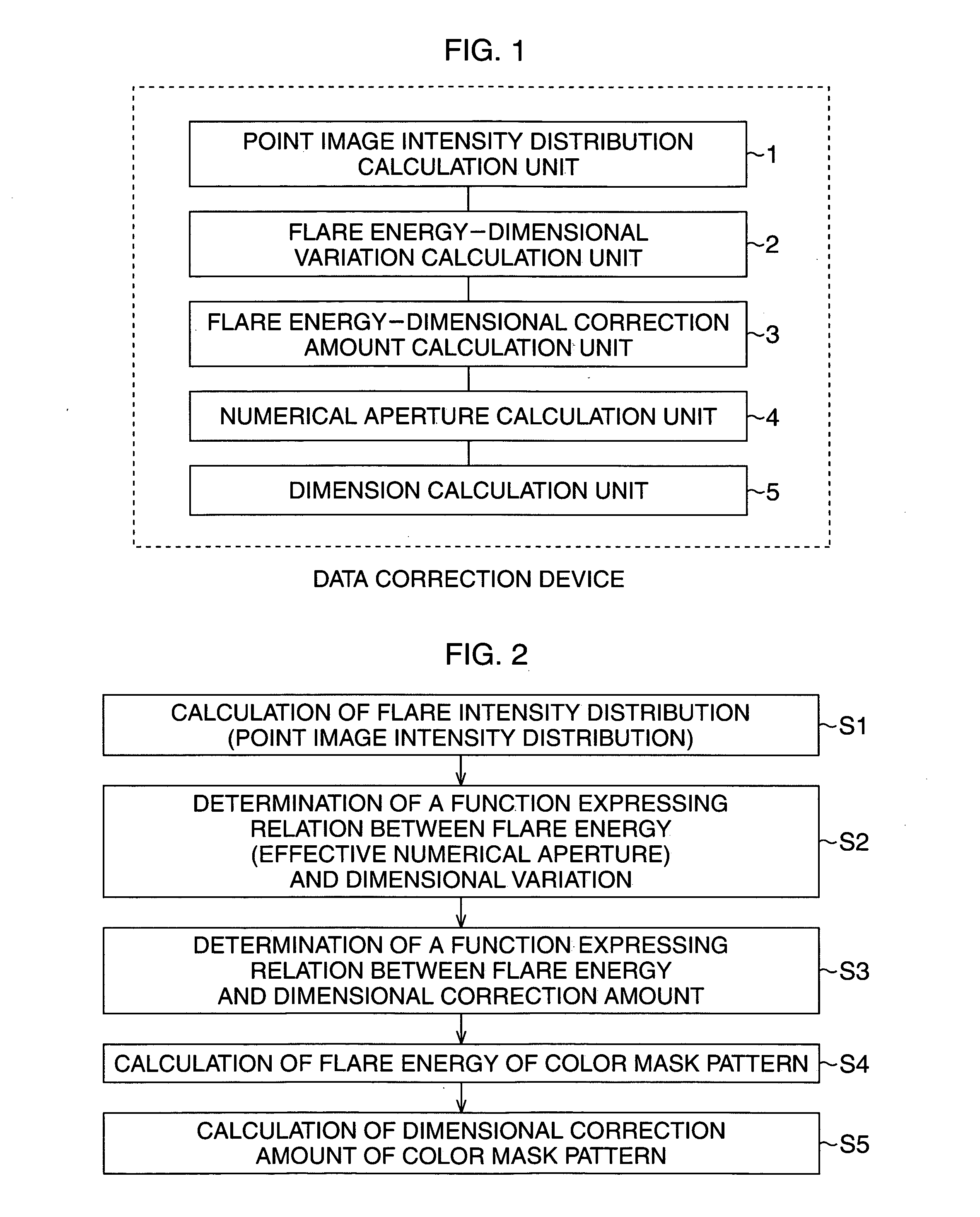
[0055]FIG. 1 is a block diagram showing a schematic configuration of a mask pattern data correction device of a first embodiment.

[0056] The data correction device is configured as having a point image intensity distribution calculation unit 1 calculating flare intensity distribution (point image intensity distribution) based on a result of dimensional measurement of a test pattern using a predetermined photomask-for-testing; a flare energy-dimensional variation calculation unit 2 calculating a relation between flare energy (effective numerical aperture) and dimensional variation using a dummy photomask adjusted in the numerical aperture; a flare energy-dimensional correction amount calculation unit 3 calculating a relation between flare energy and dimensional correction amount; a numerical aperture calculation unit 4 calculating, for every single shot region, flare energy ...

modified example 2

[0099] Next paragraphs will describe modified example 2 of the first embodiment.

[0100] The present modified example uses not only the mask pattern data of other shot regions other than the target shot region for the calculation, but uses also the mask pattern data of the chip regions other than the target chip region for the calculation.

[0101] Correction processing of design data, such as flare correction, proximity effect correction and so forth, is generally carried out respectively for every device chip region. FIG. 15A schematically shows a single shot region of an actual device, and FIG. 15B shows an enlarged view of a single chip region shown in FIG. 15A. The shot region 31 has 4×6 chip regions 111 arranged therein. A pattern of point “A” is corrected in the mask dimension thereof, by calculating flare energy from the flare region 32, which is a range (surrounded by a broken line) possibly be affected by the surrounding regions. Also a pattern of point “B” may similarly be a...

second embodiment

[0105] The present embodiment will explain light exposure correction adapted to the long-range flare.

[0106]FIG. 16 is a block diagram showing a schematic configuration of a light exposure correction device of the second embodiment.

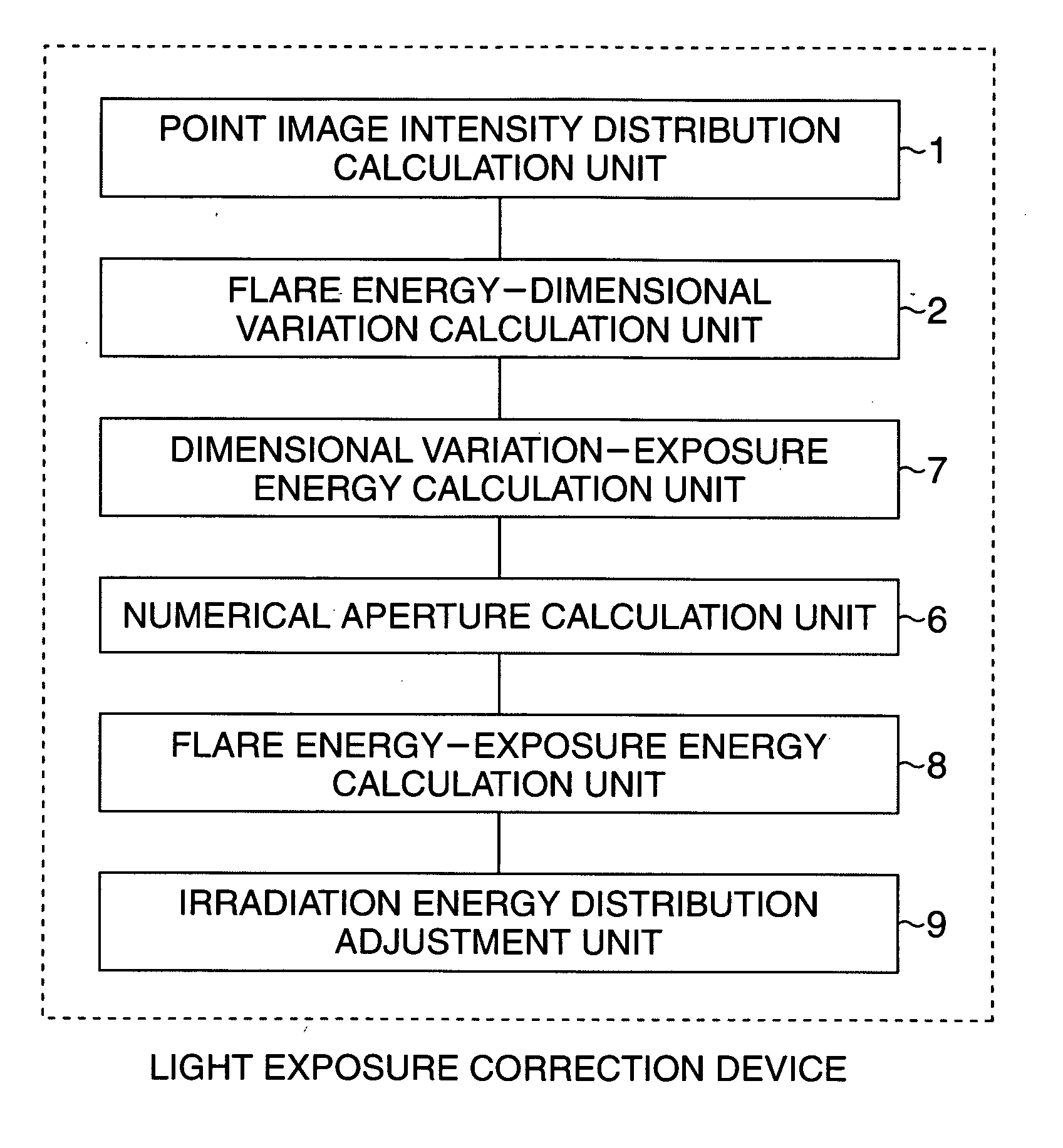
[0107] The light exposure correction device is configured as having a point image intensity distribution calculation unit 1 calculating flare intensity distribution (point image intensity distribution) based on a result of dimensional measurement of a test pattern using a predetermined photomask-for-testing; a flare energy-dimensional variation calculation unit 2 calculating a relation between flare energy (effective numerical aperture) and dimensional variation using a dummy photomask adjusted in the numerical aperture; a dimensional variation-exposure energy calculation unit 7 calculating a relation between the dimensional variation and irradiation energy (exposure energy) distribution; a numerical aperture calculation unit 4 calculating, for every sin...


PUM


Abstract

In view of realizing a lithographic process which makes it possible to estimate and correct flare with an extremely high accuracy, and causes only an extremely small dimensional variation in width, over the entire portion not only of a single shot region, but also of a single chip region, a mask pattern correction device of the present invention has a numerical aperture calculation unit calculating, for every -single shot region, flare energy for a mask pattern corresponding to a transferred pattern, based on an exposure layout of a plurality of shot regions, or more specifically, while considering flare from a plurality of shot regions located around every single shot region.

Description

CROSS-REFERENCE TO RELATED APPLICATIONS [0001] This application is based upon and claims the benefit of priority from the prior Japanese Patent Application No. 2004-216386, filed on Jul. 23, 2004, the entire contents of which are incorporated herein by reference. BACKGROUND OF THE INVENTION [0002] 1. Field of the Invention [0003] The present invention relates to a device and method for correcting mask pattern which can correct flare generated in lithographic process, one of a process step in fabrication of semiconductor devices, and also to a device and method for correcting light exposure. [0004] 2. Description of the Related Art [0005] Recent pattern formation of semiconductor devices adopts projection exposure apparatuses based on dioptric system or cata-dioptric system. In this sort of projection exposure apparatus, light ascribable to some optical routes not intended on the design basis, tends to generate due to reflection and scattering on the surface or inside of lenses in th...

Claims


Application Information

Patent Timeline
IPC IPC(8): G03C5/00G06K9/00G03F1/00G03F1/36G03F1/68H01L21/027
CPCG03F7/70433G03F7/70941G03F7/705
Inventor YAO, TERUYOSHIASAI, SATORUOSAWA, MORIMIHOSHINO, HIROMIOGINO, KOUZOUMORISHITA, KAZUMASA
Owner FUJITSU SEMICON LTD
Learn More