Method to improve inductance with a high-permeability slotted plate core in an integrated circuit

US20060022787A1Active Publication Date: 2006-02-02TEXAS INSTR INC

Image

  • Method to improve inductance with a high-permeability slotted plate core in an integrated circuit
  • Method to improve inductance with a high-permeability slotted plate core in an integrated circuit
  • Method to improve inductance with a high-permeability slotted plate core in an integrated circuit

Examples


Embodiment Construction

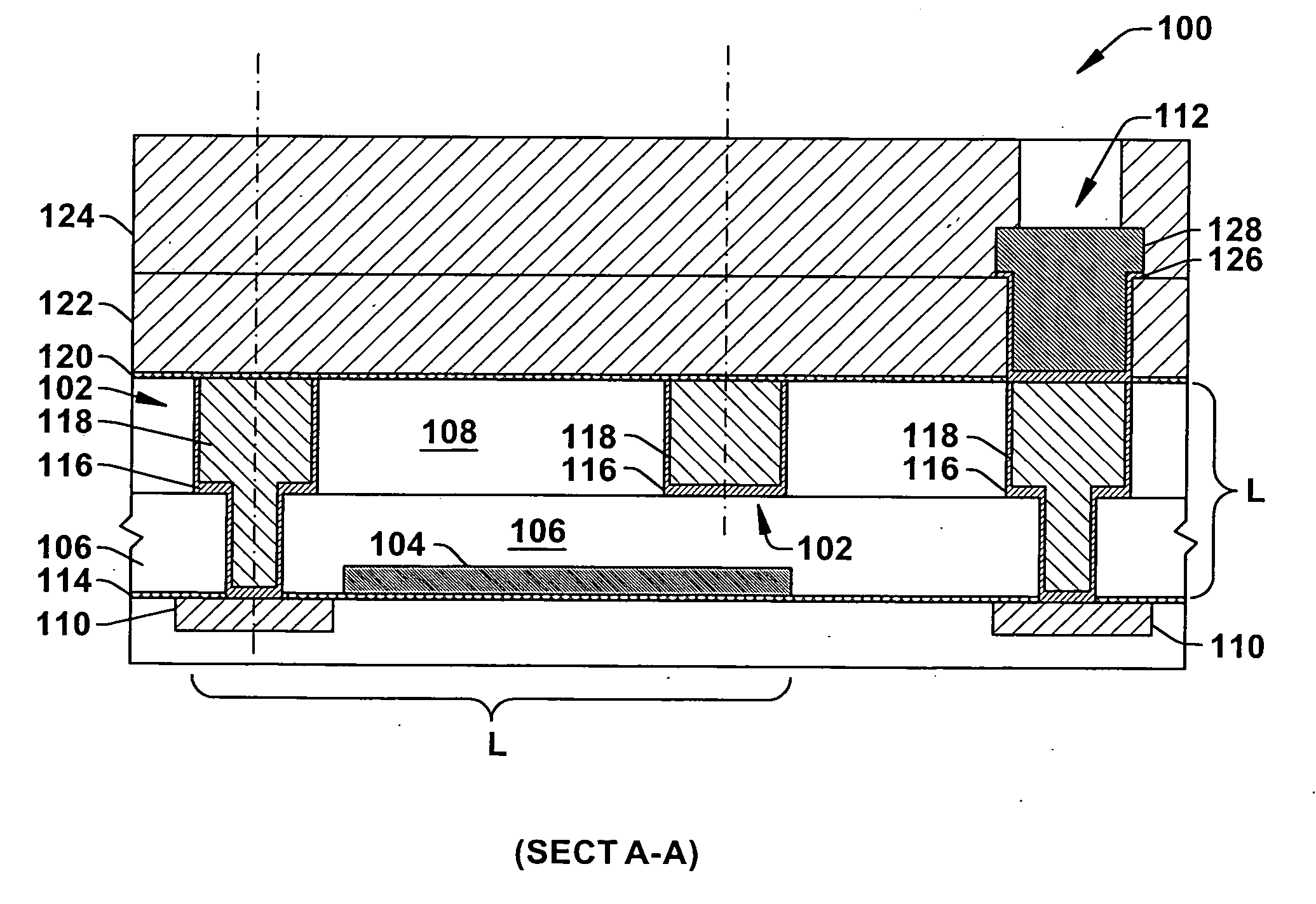
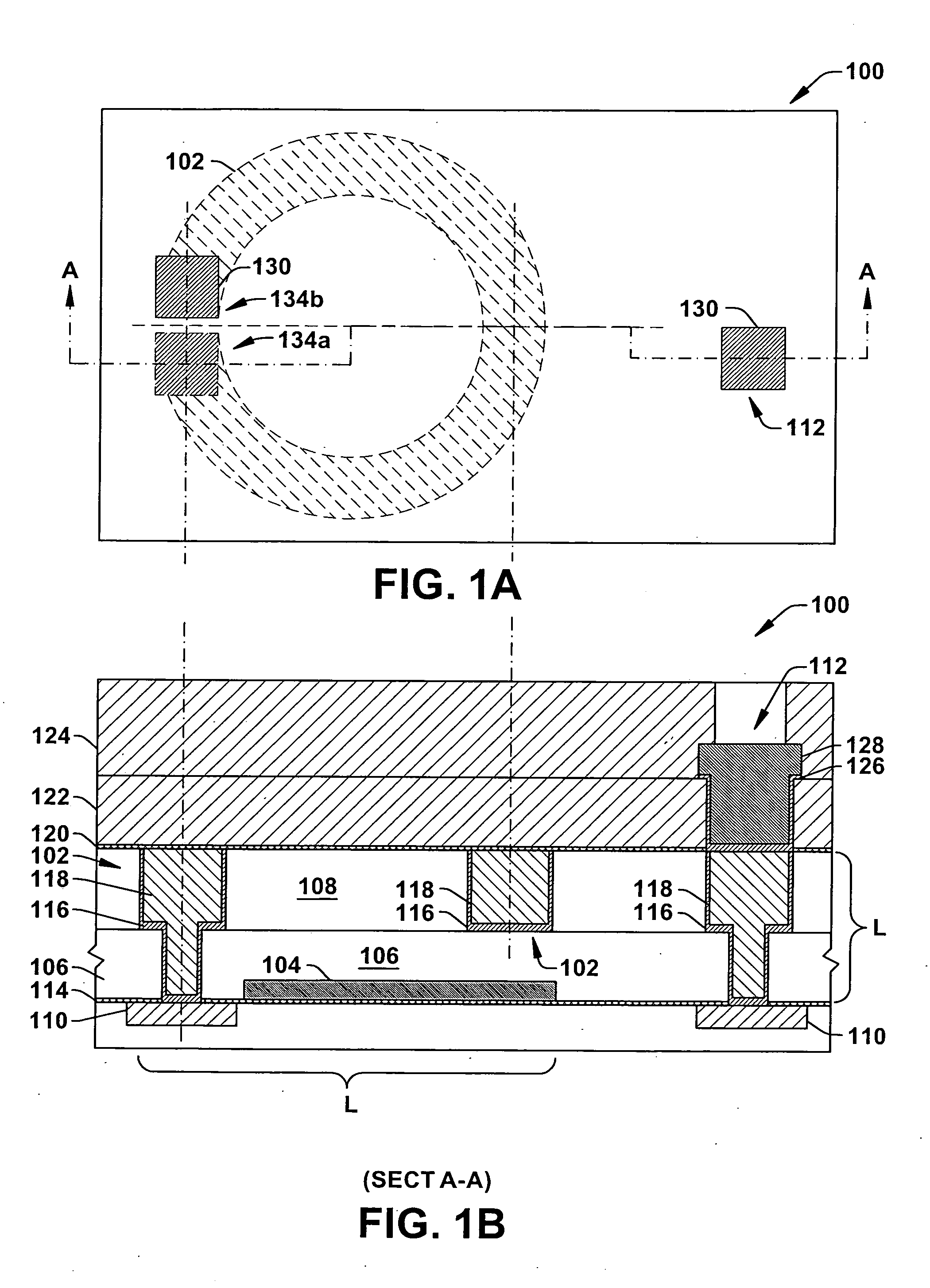
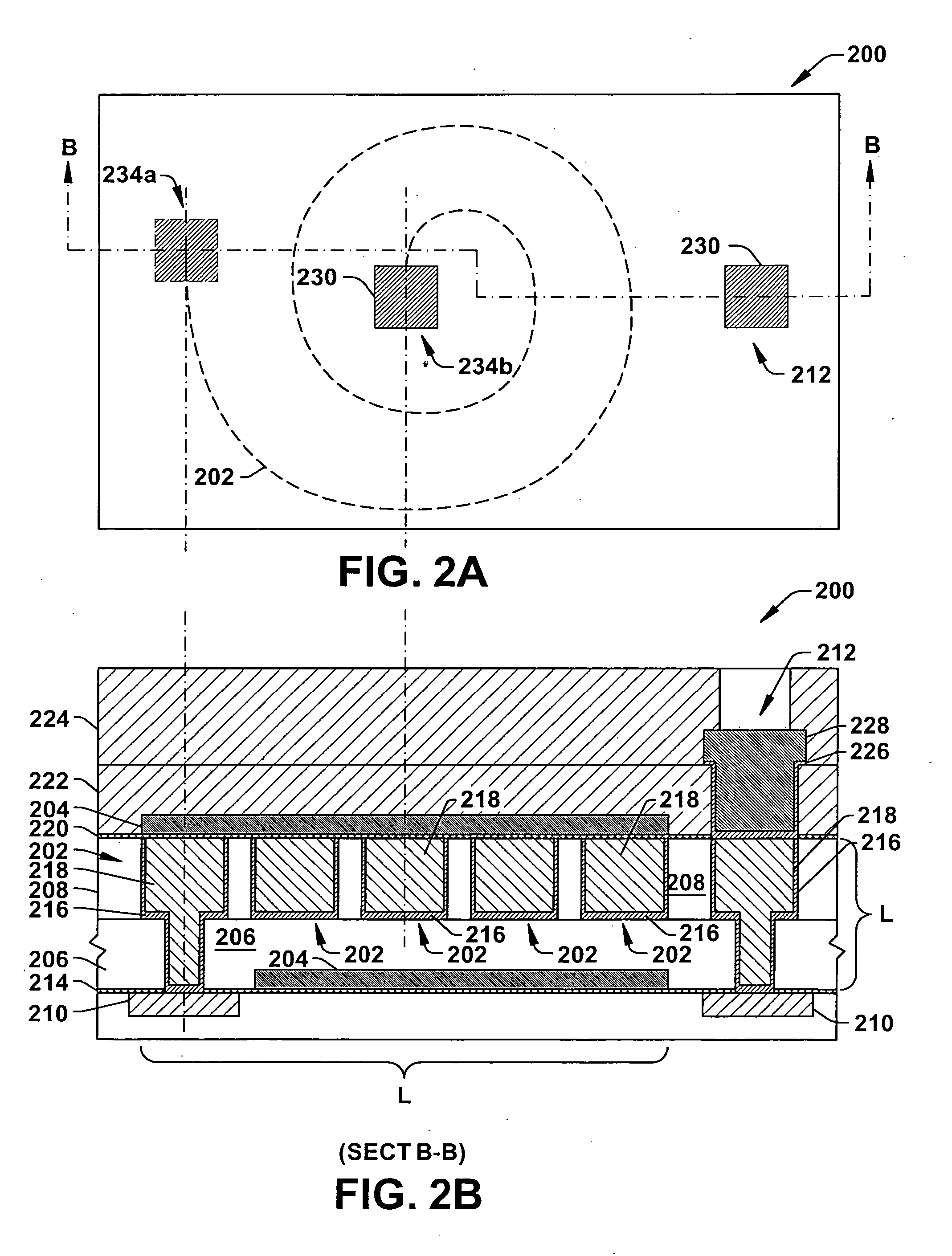
[0033] The present invention will now be described with reference to the attached drawings, wherein like reference numerals are used to refer to like elements throughout. The invention relates to an integrated inductor structure formed together with, or in close proximity to a slotted high-permeability core plate during interconnect metal level processing of integrated circuits and other devices. One or more implementations of the invention are hereinafter illustrated and described in the context of the fabrication of the integrated inductor structure and the core plate in semiconductor devices, utilizing ferromagnetic material layers, etch-stop layers, isolation layers, tantalum, and other interconnect metal or conductive layers. However, it will be appreciated by those skilled in the art, that the invention is not limited to the exemplary implementations illustrated and described hereinafter. In particular, a variety of such materials may be used to form the structures discussed. ...


PUM

PropertyMeasurementUnit
Dielectric polarization enthalpyaaaaaaaaaa
Electrical inductanceaaaaaaaaaa
Electrical conductoraaaaaaaaaa

Abstract

An inductor structure (102) formed in an integrated circuit (100) is disclosed, and includes a first isolation layer (106) and a first core plate (104) disposed over or within the first isolation layer (106, 114). The first core plate (104) includes a plurality of electrically coupled conductive traces composed of a conductive ferromagnetic material layer. A second isolation layer (108) overlies the first isolation layer and an inductor coil (102) composed of a conductive material layer (118) is formed within the second isolation layer (108). Another core plate may be formed over the coil. The one or more core plates increase an inductance (L) of the inductor coil (102).

Description

FIELD OF INVENTION [0001] The present invention relates generally to semiconductor devices and more particularly to an improved inductor formed together with one or more high permeability conductive core plates suitable for use as a plate of a planar capacitor in the fabrication of integrated circuit devices. BACKGROUND OF THE INVENTION [0002] In the manufacture of semiconductor products such as integrated circuits, individual electrical devices are formed on or in a semiconductor substrate, and are thereafter interconnected to form circuits. Interconnection of these devices within an integrated circuit is typically accomplished by forming a multi-level interconnect network in layers formed over the electrical devices, by which the device active elements are connected to other devices to create the desired circuits. Individual wiring layers within the multi-level network are formed by depositing an insulating or dielectric material layer such as SiO2 over the discrete devices or ove...

Claims


Application Information

Patent Timeline
02 Feb 2006
Publication
US20060022787A1
IPC
H01F5/00
CPC
H01F17/0006; H01F41/046; H01F2017/008; H01L23/5227; Y10T29/49073; H01L2924/0002; H01L2924/3011; H01L2924/00
Inventors
BRENNAN, KENNETH D.; PAPA RAO, SATYAVOLU S.