Method for preparing a semiconductor substrate surface for semiconductor device fabrication

a technology of semiconductor substrate and fabrication method, which is applied in the direction of semiconductor devices, basic electric elements, electrical equipment, etc., can solve the problems of poor electrical device performance, growth-related nucleation defects, and high carbon levels, and achieve the effect of improving geo2 formation

Inactive Publication Date: 2006-02-02
NORTH STAR INNOVATIONS
View PDF9 Cites 8 Cited by
  • Summary
  • Abstract
  • Description
  • Claims
  • Application Information

AI Technical Summary

Benefits of technology

[0006] According to one embodiment of the present disclosure, a method for preparing a Ge or Ge containing semiconductor substrate surface for semiconductor device fabrication including the steps of performing a first dry cleaning process, followed by a wet cleaning process, that is subsequently followed by a second dry cleaning process to rem...

Problems solved by technology

If the surface cleaning is insufficient, impurity elements such as oxygen, carbon, and metal are left over on the surface, and can lead to stacking faults or point defects, leading to poor electrical device performance.
One of these methods is a cyclic wet cleaning method which typically produces rough surfaces having high carbon levels leading to growth-related nucleation defec...

Method used


Image

  • Method for preparing a semiconductor substrate surface for semiconductor device fabrication
  • Method for preparing a semiconductor substrate surface for semiconductor device fabrication
  • Method for preparing a semiconductor substrate surface for semiconductor device fabrication

Examples


Embodiment Construction

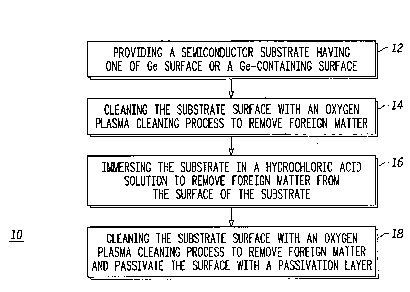
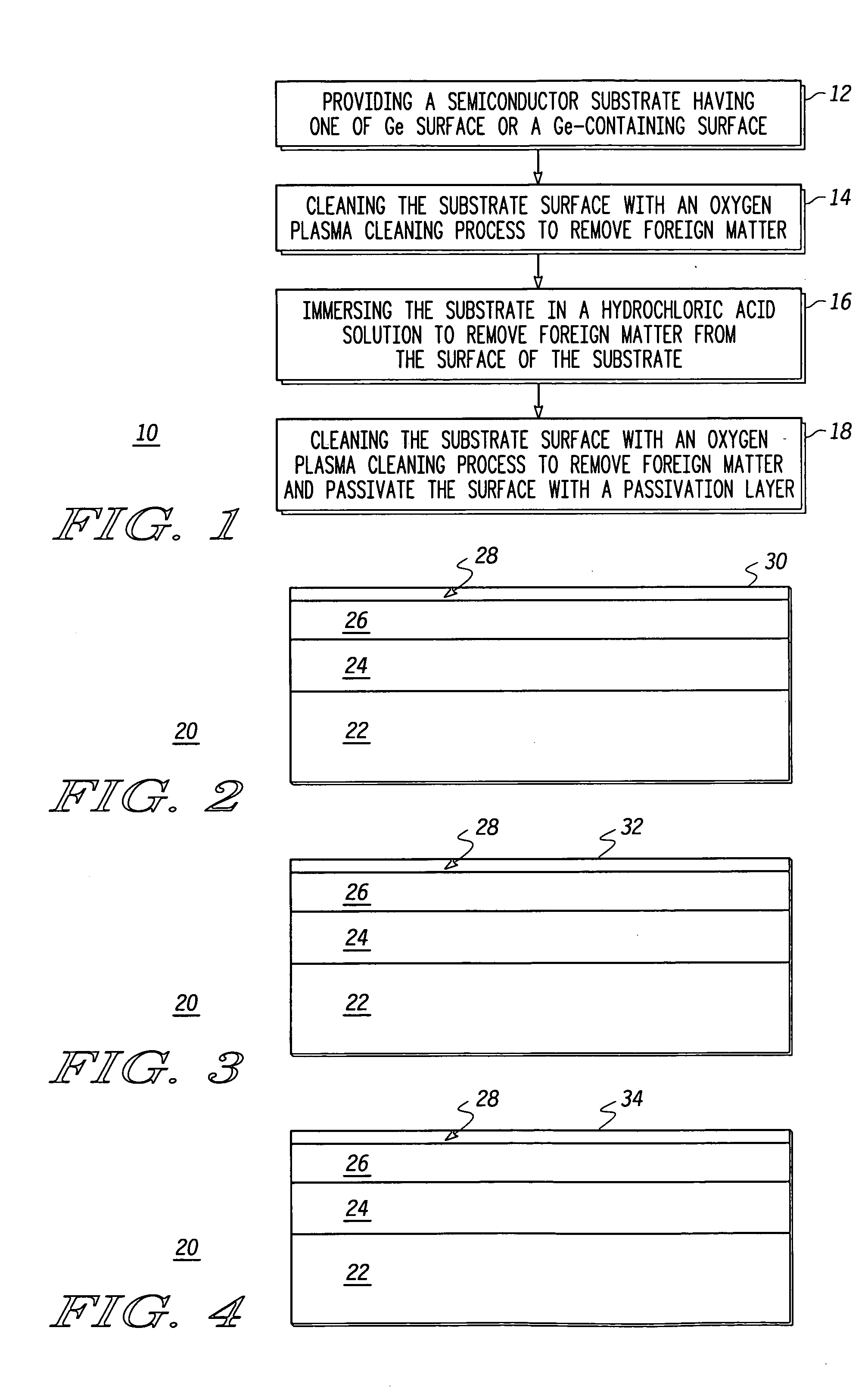
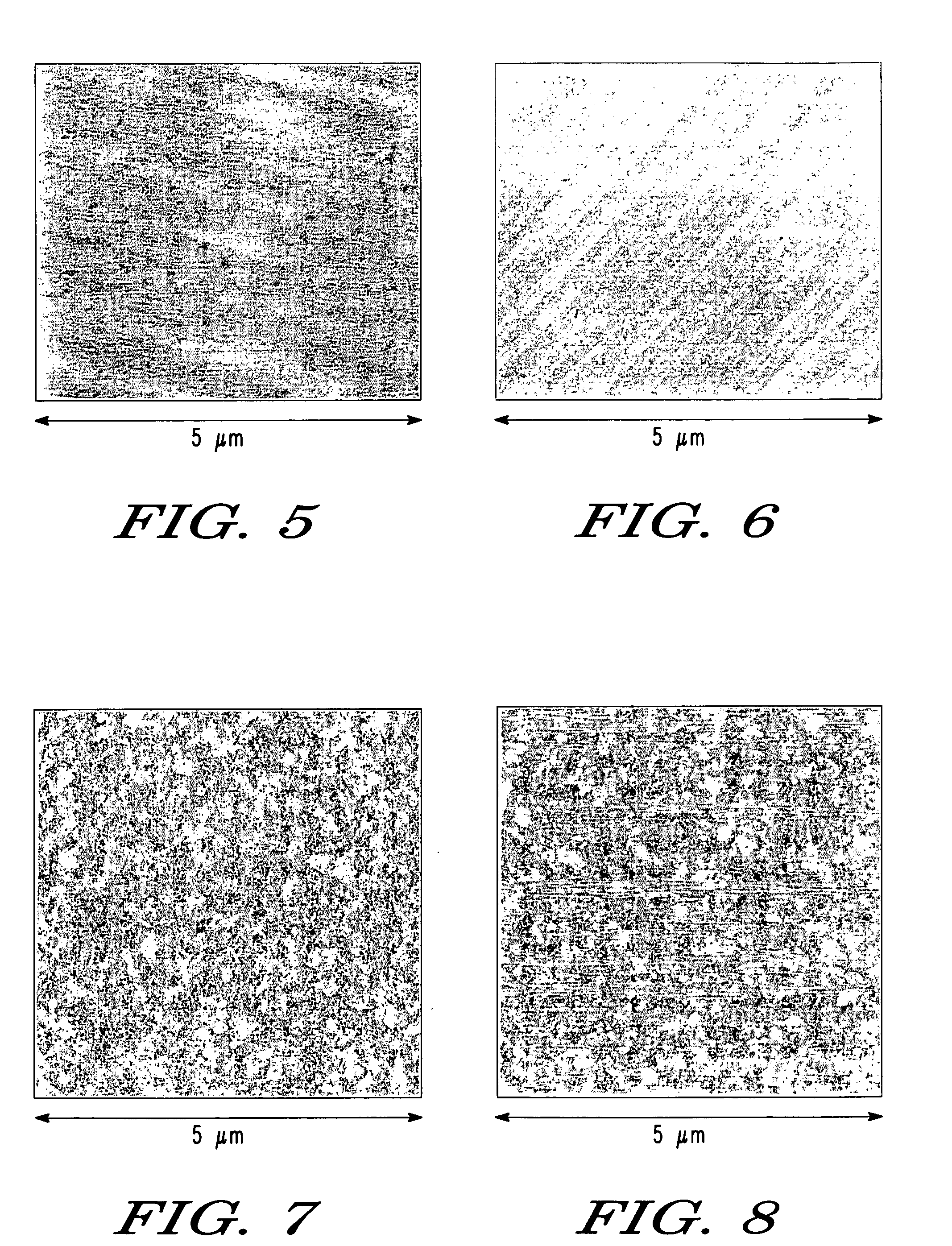
[0016] A method of preparing a germanium (Ge), or germanium (Ge)-containing, semiconductor substrate surface for the subsequent growth of epitaxial layers or a gate dielectric is disclosed. More specifically, disclosed is a new method of preparing the surface of the substrate material utilizing a three-step dry / wet / dry cleaning process to remove impurities and form an atomically smooth passivating surface layer. Accordingly, a method for preparing a Ge surface, or Ge-containing surface of a semiconductor substrate is illustrated in FIGS. 1-9.

[0017] According to an embodiment of the present disclosure, a method of preparing a Ge or Ge containing semiconductor substrate surface for epitaxial and gate dielectric growth processes provides for a dense, high purity, atomically smooth GeO2 layer on the surface.

[0018] According to an embodiment of the present disclosure, a method of preparing a Ge or Ge containing semiconductor substrate surface for epitaxial and gate dielectric growth pr...


PUM


Abstract

A method for preparing a semiconductor substrate surface (28) for semiconductor device fabrication, includes providing a semiconductor substrate (20) having a pure Ge surface layer (28) or a Ge-containing surface layer (12), such as SiGe. The semiconductor substrate (20) is cleaned using a first oxygen plasma process (14) to remove foreign matter (30) from the surface (28) of the substrate (20). The substrate surface (28) is next immersed in a hydrochloric acid solution (16) to remove additional foreign matter (30) from the surface (28) of the substrate (20). The immersion step is followed by a second oxygen plasma etch process (18), passivate the surface with a passivation layer (34), and provide for an atomically smooth surface for subsequent epitaxial or gate dielectric growth.

Description

FIELD OF THE DISCLOSURE [0001] This disclosure relates generally to a method for preparing a semiconductor substrate surface for semiconductor device fabrication. More specifically, this disclosure provides for a method for preparing a Ge or Ge-containing semiconductor substrate surface for subsequent epitaxial or gate dielectric growth. BACKGROUND OF THE DISCLOSURE [0002] Germanium surfaces, and more particularly Ge (100) surfaces, have received little attention over the past few decades due to the great success of silicon (Si) based complementary metal oxide semiconductor (CMOS) technology. There now exists a surging interest in Ge based field-effect transistors (FET) where Si cleaning techniques do not apply. This makes the preparing of Ge and / or Ge-containing surfaces for semiconductor device fabrication, such as epitaxial and gate dielectric growth processes, very important. Ge surface cleaning typically includes oxide removal, carbon removal, metallic surface contamination, an...

Claims


Application Information

Patent Timeline
IPC IPC(8): H01L21/461
CPCH01L21/02046Y10S438/906H01L21/02052
Inventor SMITH, STEVEN M.CONVEY, DIANA J.HOOPER, ANDY E.WEI, YI
Owner NORTH STAR INNOVATIONS
Why Eureka
Try Eureka