Helical microelectronic contact and method for fabricating same

a microelectronic contact and helical technology, applied in the direction of coupling device connection, semiconductor/solid-state device details, instruments, etc., can solve the problems of manufacturing equipment and process time, the cost of fine-pitch spring contact fabrication has limited the range of applicability of less cost-sensitive applications, and the inability to readily re-use the solder ball connection, etc., to achieve the effect of saving substantial processing time during the plating step

Inactive Publication Date: 2006-02-02
FORMFACTOR INC
View PDF26 Cites 6 Cited by
  • Summary
  • Abstract
  • Description
  • Claims
  • Application Information

AI Technical Summary

Benefits of technology

[0023] Where compliant instead of sacrificial pads are used, the support of the compliant material may enable use of a thinner plated layer for the spring contacts than would otherwise be required to provide adequate contact forces. The thinner plated layer, in turn, may save substantial processing time during the plating step. Also, the foregoing method avoids any need for contouring or molding of a sacrificial layer, any need for separate forming steps for providing a sharp contact tip, and any need for a separate step to provide redistribution traces.

Problems solved by technology

Once melted and re-hardened, the solder ball connections cannot readily be re-used, if at all.
Presently, however, the cost of fabricating fine-pitch spring contacts has limited their range of applicability to less cost-sensitive applications.
Much of the fabrication cost is associated with manufacturing equipment and process time.
One key disadvantage is the requirement for a polymer underfill beneath a die.
The presence of the underfill often makes it infeasible to rework the component.
This design lacks an elastomer layer for decoupling the die from the PCB and, therefore, may not eliminate the need for underfill.
The elastomeric materials tend to absorb moisture, and if excessive moisture is absorbed, rapid outgassing of this moisture at reflow temperatures may cause the formation of voids in the elastomer layer, or bursting of the package.
For example, moisture may be released from polymer materials in the elastomer and become trapped within the die attachment adhesive.
Voids may then be formed when this trapped moisture expands during board assembly heating operations, typically causing cracking and package failure.
Formation of such voids may be particularly problematic during reflow attachment to a PCB.
Another difficulty with chip-scale package designs is the process for integrating the elastomer member, which is typically done by picking and placing elastomer pads onto individual sites, or by screen printing and subsequently curing a fluid polymer.
In either case, it may be difficult to meet the tight tolerances and package flatness required for a CSP application.
This level of flatness may be difficult to achieve using prior art processes for depositing the elastomeric materials.

Method used


Image

  • Helical microelectronic contact and method for fabricating same
  • Helical microelectronic contact and method for fabricating same
  • Helical microelectronic contact and method for fabricating same

Examples


Embodiment Construction

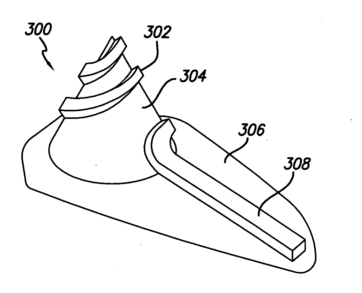
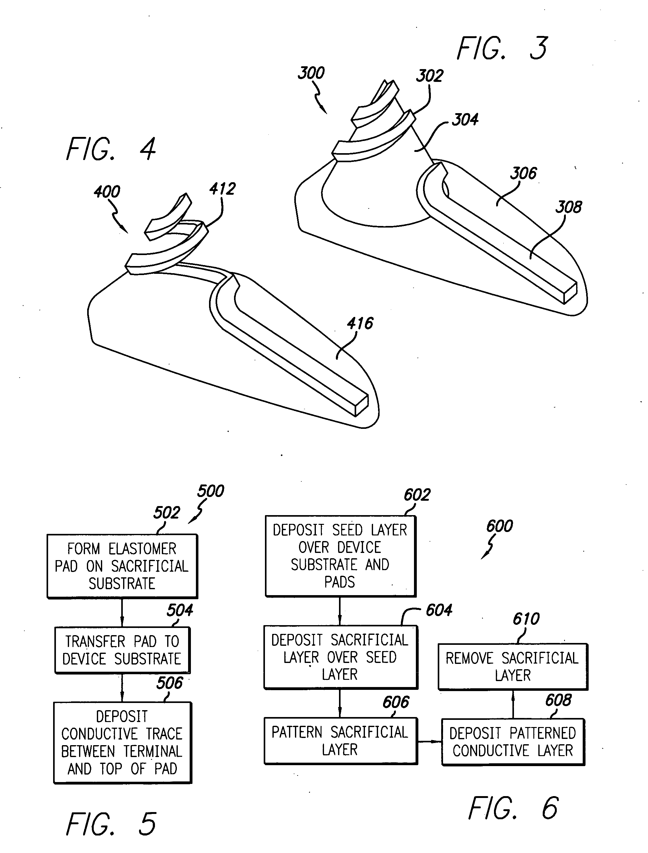
[0036] The present invention provides microelectronic spring contacts that overcome limitations of prior art spring contacts. In the detailed description that follows, like element numerals are used to describe like elements appearing in one or more of the figures.

[0037] The present invention achieves the benefits of multi-layer and single-layer lithographic spring contacts as disclosed in the patent applications referenced herein, at a potentially lower cost, and provides additional advantages for certain packaging and connecting applications. The spring contacts of the present invention are believed especially suitable for compact packaging applications, such as flip-chip packages and CSP's, where they may replace or augment the use of ball grid arrays as connection elements.

[0038] With proper selection of materials, the spring contacts may also be used for testing and burn-in applications. It is therefore within the scope and intent of the invention that spring contacts accordi...


PUM


Abstract

A microelectronic spring contact for making electrical contact between a device and a mating substrate and method of making the same are disclosed. The spring contact has a compliant pad adhered to a substrate of the device and spaced apart from a terminal of the device. The compliant pad has a base adhered to the substrate, and side surfaces extending away from the substrate and tapering to a smaller end area distal from the substrate. A trace extends from the terminal of the device in a coil pattern over the compliant pad to its end area, forming a helix. At least a portion of the compliant pad end area is covered by the trace, and a portion of the trace that is over the compliant pad is supported by the compliant pad. In an alternative embodiment, the pad is removed to leave a freestanding helical contact.

Description

BACKGROUND OF THE INVENTION [0001] 1. Field of the Invention [0002] The present invention relates to microelectronic contacts for use with semiconductor devices and the like. [0003] 2. Description of Related Art [0004] The demand for ever-smaller and more sophisticated electronic components has driven a need for smaller and more complex integrated circuits (ICs). The ever-smaller ICs and high lead counts, in turn, require more sophisticated electrical connection schemes, both in packaging for permanent or semi-permanent attachment, and for readily demountable applications such as testing and burn-in. [0005] For example, many modern IC packages have smaller footprints, higher lead counts and better electrical and thermal performance than IC packages commonly used only a few years ago. One such compact IC package is the ball grid array (BGA) package. A BGA package is typically a rectangular package with terminals, normally in the form of an array of solder balls, protruding from the b...

Claims


Application Information

Patent Timeline
Patent Type & Authority Applications(United States)
IPC IPC(8): H01R12/00G01R1/067G01R31/28H01L21/48H01L23/498H01R4/48H01R13/03H01R13/24H01R13/33H01R43/16H05K3/32H05K3/40
CPCG01R1/06711G01R1/06744G01R31/2884H01L21/4853H01L23/49811H01R4/4863H01R12/57H01R13/035H01R13/2421H01R13/33H01R23/72H01R43/16H05K3/326H05K3/4007H05K3/4092H05K2201/0133H05K2201/0367H05K2201/10265H05K2203/308H01L2224/16G01R1/06733H01L2924/00014H01L2224/0401H01L23/48H01L23/485
Inventor LINDSEY, SCOTT E.MILLER, CHARLES A.ROYSTER, DAVID M.WENZEL, STUART W.
Owner FORMFACTOR INC
Why Eureka
Try Eureka