
Light irradiation apparatus, crystallization apparatus, crystallization method and device

a technology of crystallization apparatus and light irradiation apparatus, which is applied in the field of light irradiation apparatus, crystallization apparatus, crystallization method and device, can solve the problems of deteriorating transistor characteristics, uneven display, and destruction of semiconductor films, and achieve the effect of high filling ratio

Inactive Publication Date: 2006-02-09
ADVANCED LCD TECH DEVMENT CENT
View PDF0 Cites 4 Cited by
  • Summary
  • Abstract
  • Description
  • Claims
  • Application Information

AI Technical Summary

Benefits of technology

[0019] It is an object of the present invention to provide a technique which can stably form a desired light intensity distribution with an inverse peak shape at a desired position and form a crystal grain to a semiconductor film with a high filling ratio.
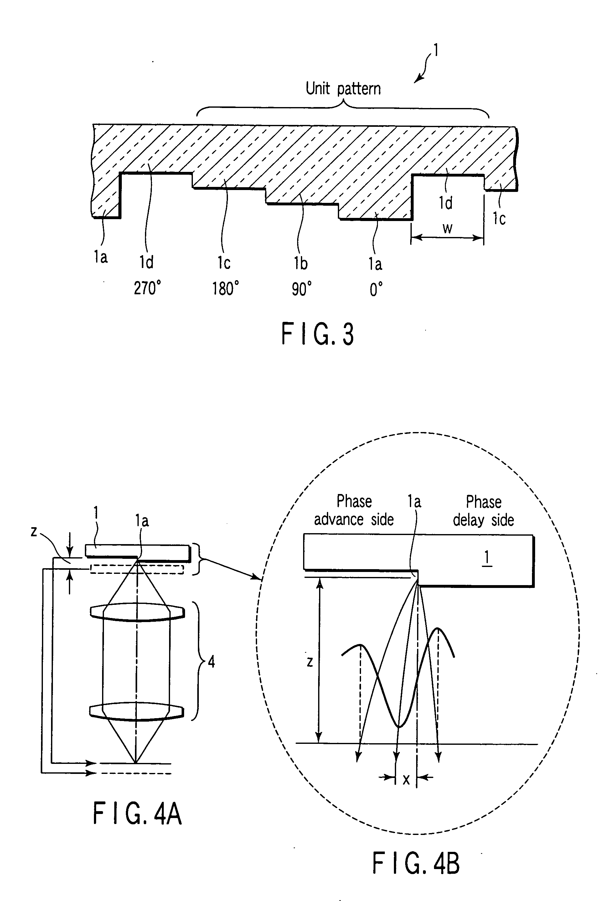
[0030] In the crystallization apparatus according to the typical mode of the present invention, since a light modulation element is illuminated with an illumination light beam inclined in a direction crossing a step line of a phase step of the light modulation element, even if a light modulation element which has a phase step having a phase difference substantially different from 180°, the symmetry of, e.g., a light intensity distribution with an inverse peak shape can be excellently maintained without being dependent on a defocus direction, and hence a deep depth of focus can be realized. As a result, in the present invention, a desired light intensity distribution with an inverse peak shape can be stably formed at a desired position, and a crystal grain can be formed to a semiconductor film with a high filling ratio.

Problems solved by technology

Additionally, each of many thin-film transistors formed by using polysilicon has a different number of crystal grain boundaries formed in its channel portion, and this difference becomes irregularities, resulting in a problem of unevenness in display in case of a liquid crystal display.
Furthermore, since a position of the bottom peak is shifted in a plane by defocusing, a position of a crystal grain to be generated is also shifted from a desired position, which becomes a problem when forming a circuit by using this crystal grain.
That is, when a crystal grain is not formed at a desired position, a boundary or boundaries of crystal grains exist in a channel portion of a transistor, thereby deteriorating characteristics of the transistor.
As a result, there is an inconvenience that a semiconductor film is destroyed due to ablation at this peak position on one side.

Method used


Image

  • Light irradiation apparatus, crystallization apparatus, crystallization method and device
  • Light irradiation apparatus, crystallization apparatus, crystallization method and device
  • Light irradiation apparatus, crystallization apparatus, crystallization method and device

Examples


Embodiment Construction

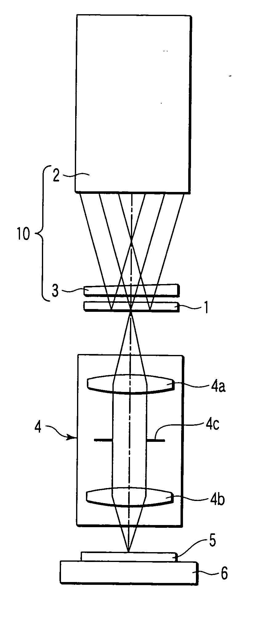
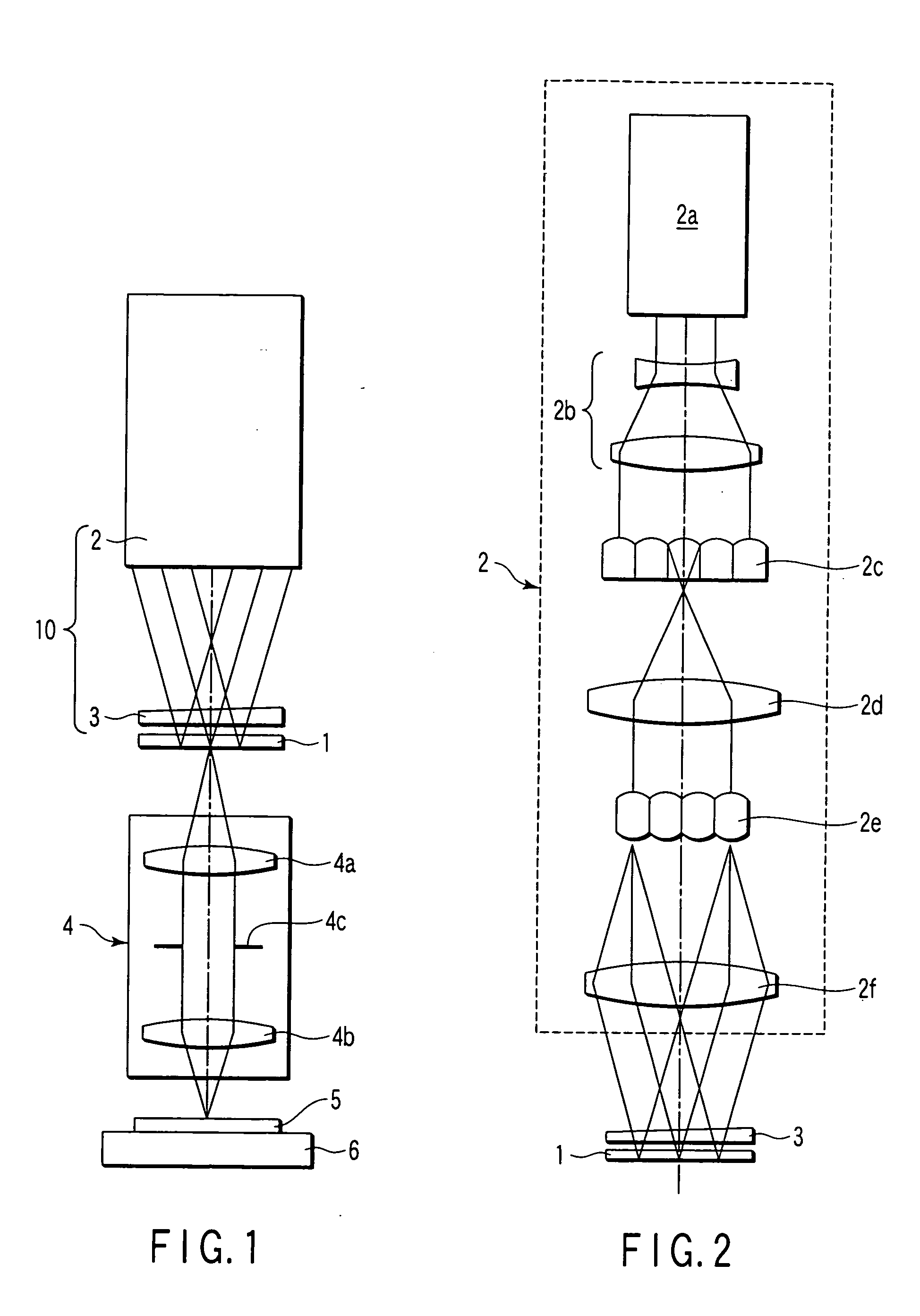
[0051] A mode of the present invention will now be described based on the accompanying drawings. FIG. 1 is a view schematically showing a configuration of a crystallization apparatus according to the mode of the present invention. Further, FIG. 2 is a view schematically showing an internal configuration of an illumination optical system depicted in FIG. 1. Referring to FIGS. 1 and 2, the crystallization apparatus according to this mode comprises a phase shifter (a light modulation element) 1 which forms a light beam having a predetermined light intensity distribution by modulating a phase of an incident light beam, an illumination optical system 10 which illuminates the phase shifter, an image formation optical system 4, and a substrate supporting stage 6 which holds a processed substrate 5.

[0052] As shown in FIG. 3, the phase shifter 1 is constituted by repeatedly arranging unit patterns in a lateral direction (in a right-and-left direction in the figure). The unit pattern include...


PUM

PropertyMeasurementUnit
wavelengthaaaaaaaaaa
incidence angleaaaaaaaaaa
wavelengthaaaaaaaaaa

Abstract

A light irradiation apparatus includes a light modulation element which has a phase step having a phase difference substantially different from 180°, an illumination optical system which illuminates the light modulation element, and an image formation optical system which forms, on an irradiation surface, a light intensity distribution based on a light beam phase-modulated by the light modulation element. The illumination optical system illuminates the light modulation element with an illumination light beam inclined in a direction normal to a step line of the phase step.

Description

CROSS-REFERENCE TO RELATED APPLICATIONS [0001] This application is based upon and claims the benefit of priority from prior Japanese Patent Application No. 2004-232708, filed Aug. 9, 2004, the entire contents of which are incorporated herein by reference. BACKGROUND OF THE INVENTION [0002] 1. Field of the Invention [0003] The present invention relates to a light irradiation apparatus, a crystallization apparatus, a crystallization method and a device. In particular, the present invention relates to a crystallization apparatus and a crystallization method which generate a crystallized semiconductor film by irradiating a non-single-crystal semiconductor film with a laser light having a predetermined light intensity distribution. [0004] 2. Description of the Related Art [0005] A thin film transistor (TFT) used for a switching element or the like which selects a display pixel in, e.g., a liquid crystal display (LCD) has been conventionally formed by using amorphous silicon or polysilico...

Claims


Application Information

Patent Timeline
Patent Type & Authority Applications(United States)
IPC IPC(8): G21G5/00
CPCB23K26/0656H01L21/2026G03F7/70283G03F1/34Y10S117/904B23K26/066H01L21/02686H01L21/02422H01L21/02488H01L21/02502H01L21/02678H01L21/02598H01L21/02532H01L21/324H01L21/02
Inventor TANIGUCHI, YUKIOMATSUMURA, MASAKIYO
Owner ADVANCED LCD TECH DEVMENT CENT
Learn More