

Method of manufacturing semiconductor device
a manufacturing method and semiconductor technology, applied in the direction of semiconductor devices, basic electric elements, electrical appliances, etc., can solve the problems of deterioration of high-frequency characteristics, increased process load, and inability to obtain desired withstanding characteristics, so as to reduce the step of using a thermal oxidation method and achieve the effect of reducing the occurrence of crystal defects in the semiconductor layer in the lower edge portion, reducing the electric field concentration, and reducing the step of using a thermal oxidation
- Summary
- Abstract
- Description
- Claims
- Application Information
AI Technical Summary
Benefits of technology
Problems solved by technology
Method used
Image

Examples
Embodiment Construction
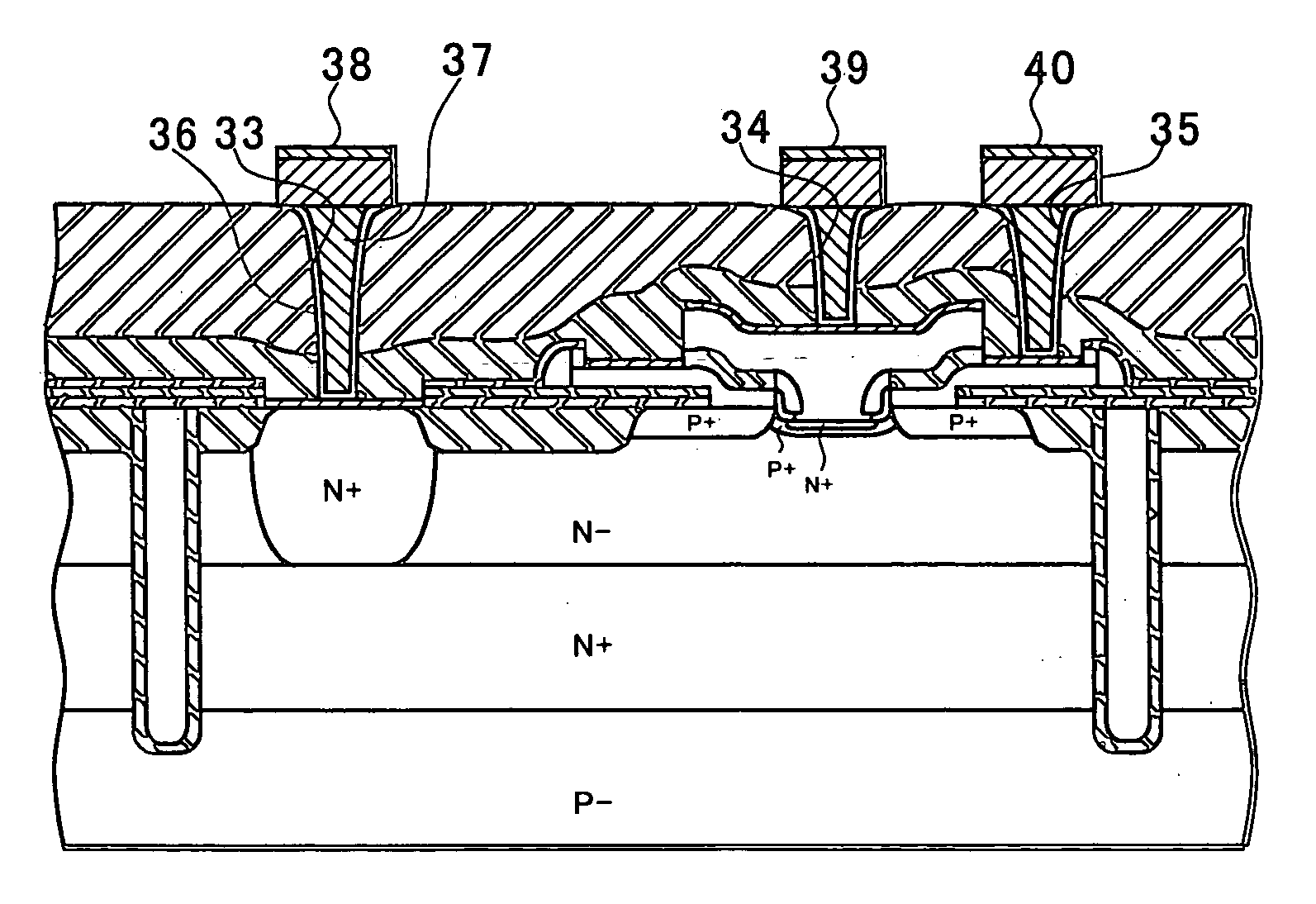
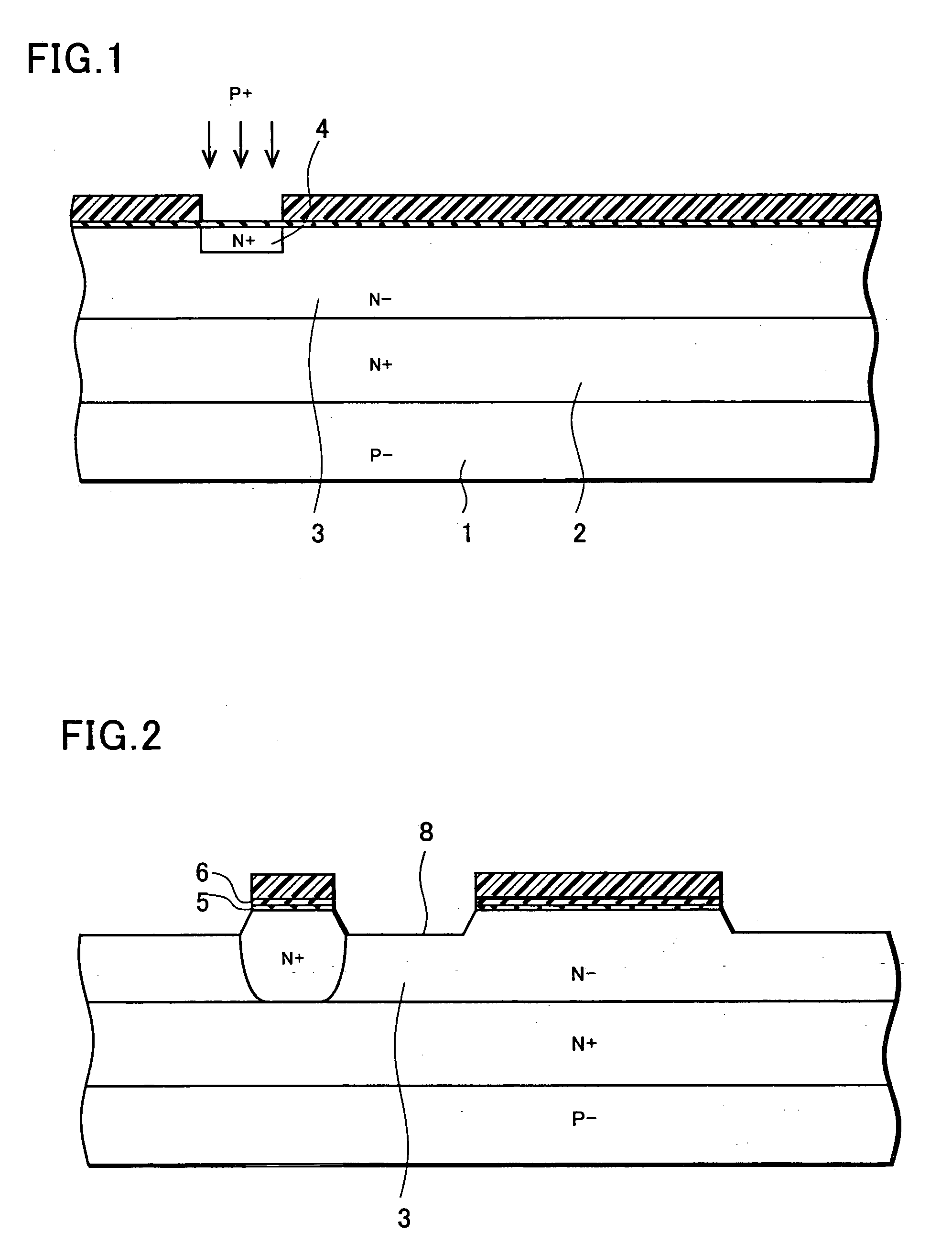
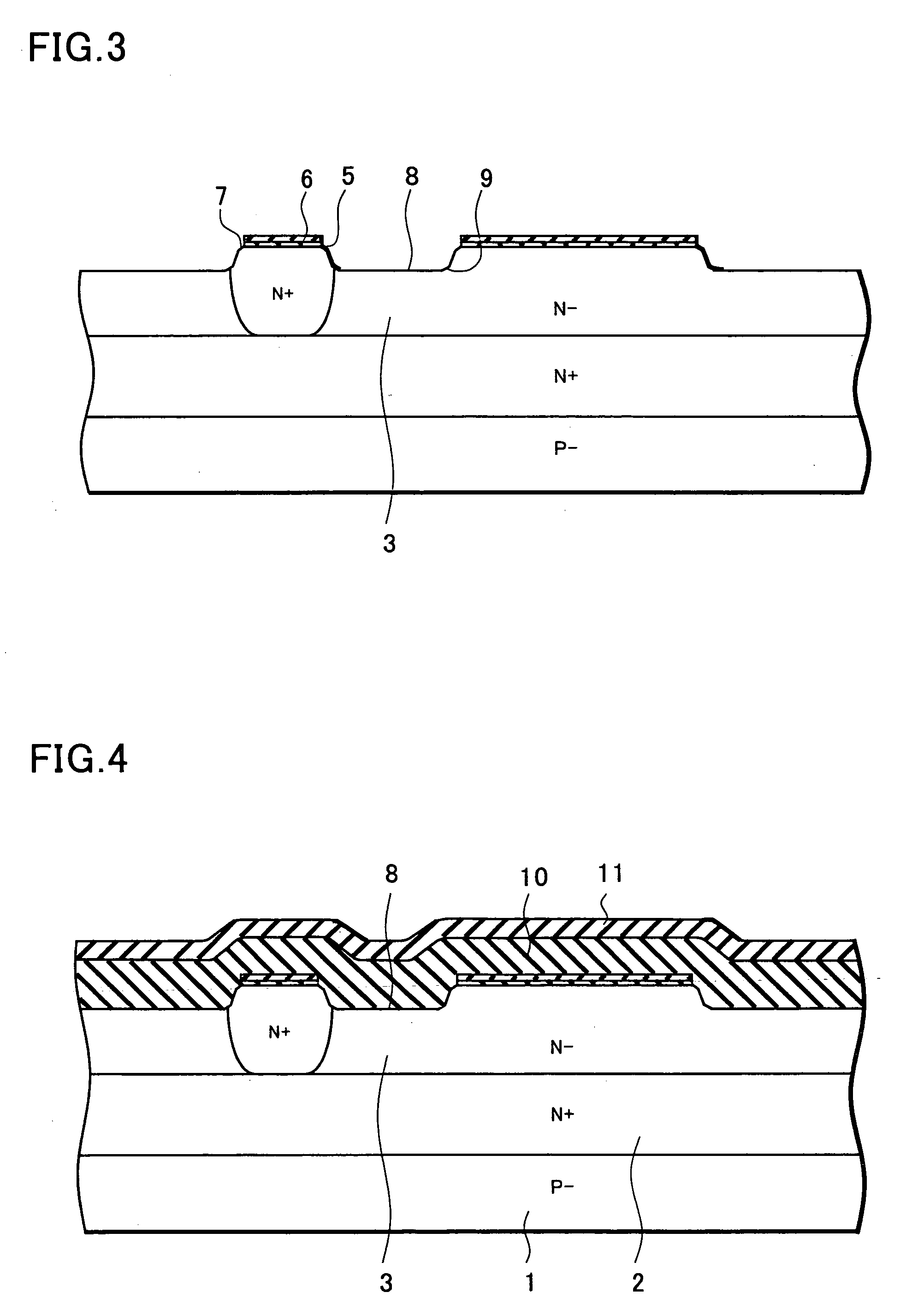
[0030] With reference to FIGS. 1 to 12, a method of manufacturing a semiconductor device according to a preferred embodiment of the invention will be described in detail below.
[0031] FIGS. 1 to 12 are cross-sectional views showing the method of manufacturing a semiconductor device according to this embodiment. Note that, although a case where an NPN-type transistor, for example, is formed in one of element formation regions separated by isolation regions will be described in the following description, the embodiment of the present invention is not limited to this case. For example, a semiconductor integrated circuit device may be formed by forming an N-channel MOS transistor, a P-channel MOS transistor, a vertical PNP transistor and the like in the other element formation regions.
[0032] First, as shown in FIG. 1, a P-type single crystal silicon substrate 1 is prepared. By use of a heretofore known photolithography technology, an N-type buried diffusion layer 2 is formed on a surfa...
PUM
 Abstract
Description
Claims
Application Information