Low-voltage, solid-state, ionizing-radiation detector

a detector and solid-state technology, applied in the direction of radiation measurement, instruments, electrical equipment, etc., can solve the problem of not providing information regarding the depth of penetration of incident radiation into the detector material, and achieve the effect of improving manufacturing flexibility, reducing operating voltage, and increasing detector safety

Inactive Publication Date: 2006-02-16
V TARGET TECH
View PDF10 Cites 24 Cited by
  • Summary
  • Abstract
  • Description
  • Claims
  • Application Information

AI Technical Summary

Benefits of technology

[0011] The present invention successfully addresses the shortcomings of presently known configurations by providing a stratified, solid-state detector for ionizing radiation, wherein an operating bias is applied in parallel to all the strata. Since the bias required for accelerating electrons away from holes in a solid-state material is generally a function of material thickness, a stack of thin solid-state-material layers, connected in parallel, will operate at only a fraction of the bias required for a single, thick layer of solid-state-material of an equivalent thickness. Thus, stratification allows for reduced operating voltage and improved manufacturing flexibility. Additionally, a high-voltage power supply need not be used, thus increasing the safety of the detector. Stratification may further provide information on incident-radiation energy, based on depth penetration into the detector, wherein the layers may operate as “depth pixels.” Generally, the higher the incident radiation energy, the greater the probability for deep pe

Problems solved by technology

Nonetheless, present-day solid-state detectors for ionizing radiation operate at a relatively high bias, so as to affect both the cost and the overall volum

Method used


Image

  • Low-voltage, solid-state, ionizing-radiation detector
  • Low-voltage, solid-state, ionizing-radiation detector
  • Low-voltage, solid-state, ionizing-radiation detector

Examples


first embodiment

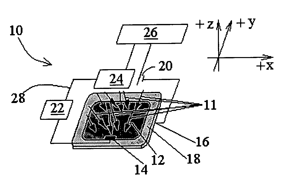
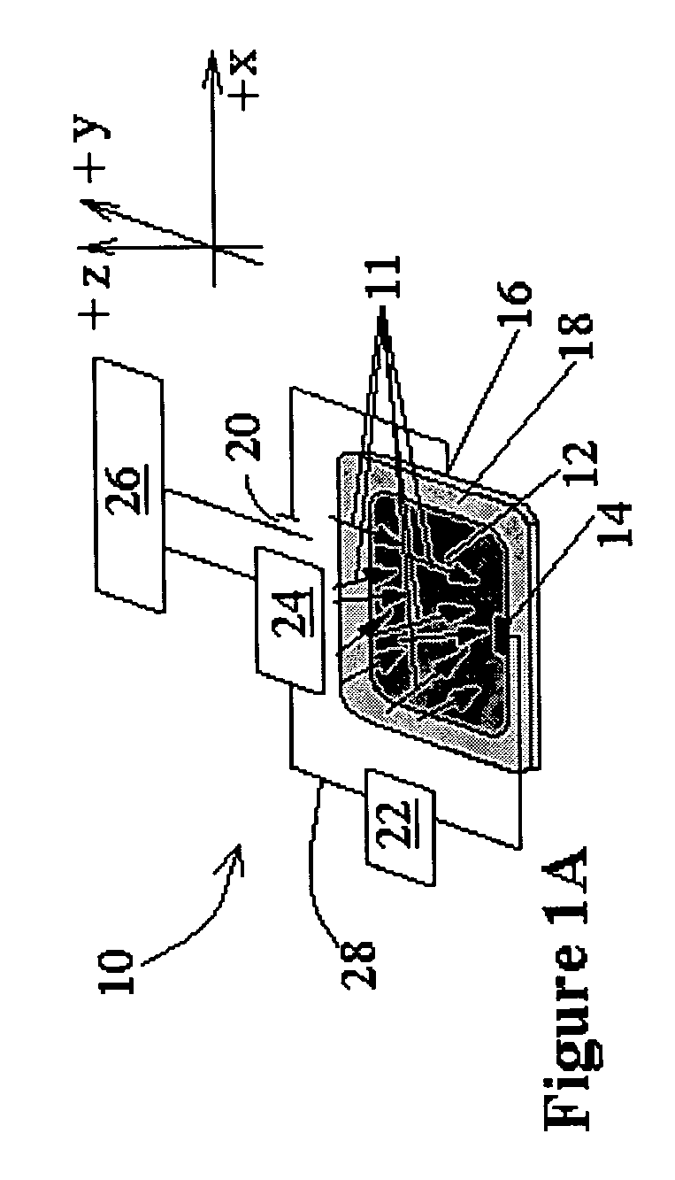
[0073]FIG. 2A schematically illustrates a stratified, single-pixel, solid-state detector 40, in accordance with the present invention. The stratified, single-pixel, solid-state detector 40 comprises at least two, and preferably a plurality of solid-state-material layers 42(K), along the x;y plane of the x;y;z coordinate system, so as to form a stack 67. A layer thickness, in the z direction, may be between about 0.5 and 1 mm, yet, thinner layers may be used where practical to manufacture.

[0074] The solid-state-material layers 42(K) are arranged, for example, for detecting the ionizing radiation 11 incident on the x;y plane and have positive and negative electrode connections 44(K) and 46(K), respectively, wherein negative connections 46(K) may be common, and regarded simply as negative connections 46. Preferably, each of the solid-state-material layers 42(K) is surrounded by the insulation material 18. Preferably, each of the solid-state-material layers 42(K) is associated with a pr...

second embodiment

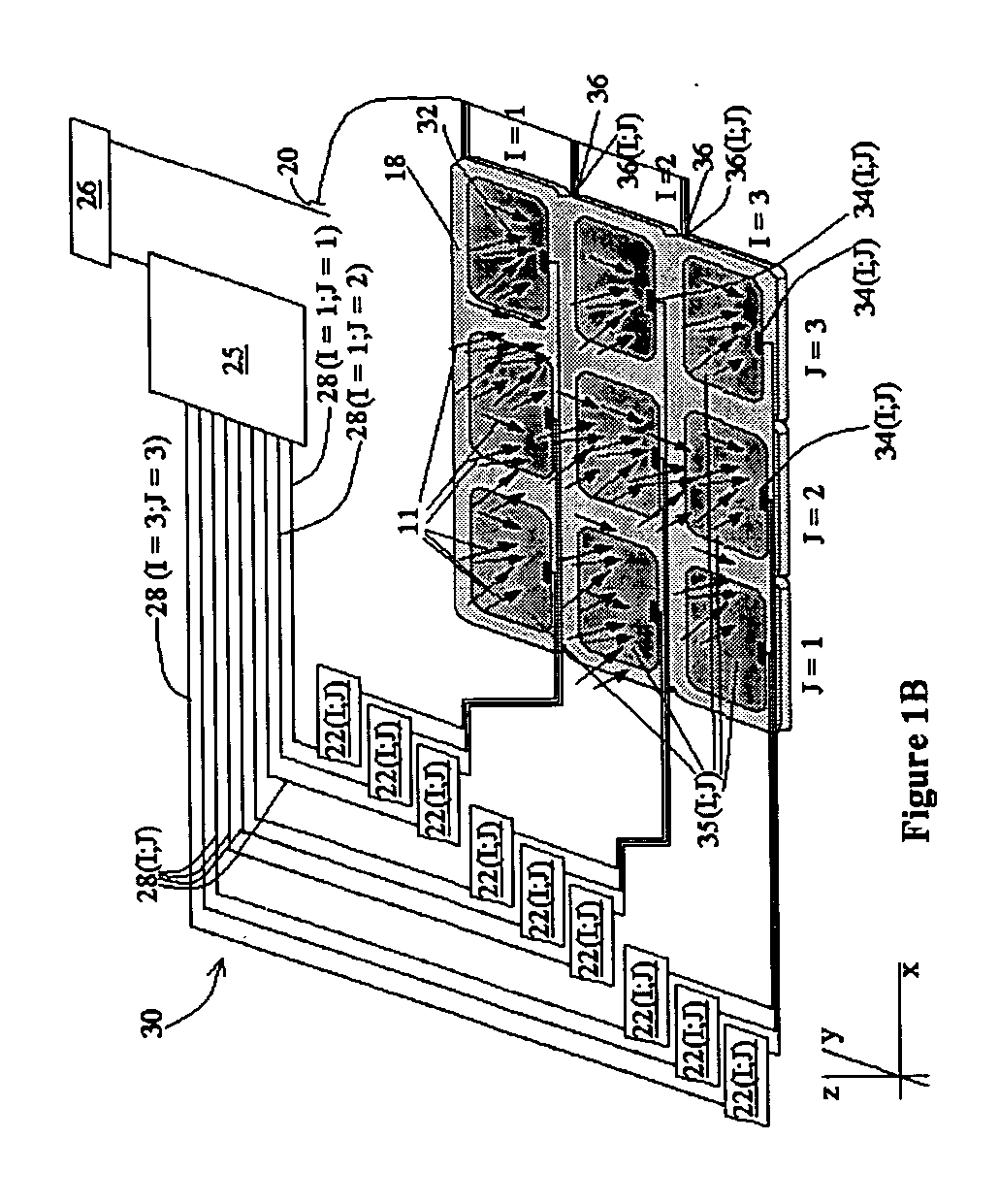
[0081]FIG. 2C schematically illustrates a single-pixel, solid-state detector 50, in accordance with the present invention, wherein layers 42(K) may be thought of as “depth pixels.” Accordingly, wires 28(K), associated with layers 42(K), lead to a multi-channel counter 25, wherein each layer 42(K) is assigned a channel. In this manner, information on the incident radiation energy may be obtained, since generally, the higher the incident radiation energy, the greater the depth of penetration into the detector material.

[0082] Each of the solid-state-material layers 42(K) may be, for example, a square, in the x;y plane, having sides of between about 3 mm and about 10 mm. It will be appreciated that other dimensions may similarly be used. It will be further appreciated that another polygon, a circle, or another geometrical shape may be used.

[0083] The solid-state-material layers 42(K) may be, for example, room temperature CdZnTe. Alternatively, CdTe, HgI, Si, Ge, or the like may be used...


PUM


Abstract

A stratified, solid-state detector for ionizing radiation, is provided, wherein an operating bias is applied in parallel to all the strata. Since the bias required for accelerating electrons away from holes in a solid-state material is generally a function of material thickness, a stack of thin solid-state-material layers, connected in parallel, will operate at only a fraction of the bias required for a single, thick layer of solid-state-material of an equivalent thickness. Thus, stratification allows for reduced operating voltage and improved manufacturing flexibility. Additionally, a high-voltage power supply need not be used, thus increasing the safety of the detector. Stratification may further provide information on incident-radiation energy, based on depth penetration into the detector, wherein the layers may operate as “depth pixels.” Generally, the higher the incident radiation energy, the greater the probability for deep penetration into the solid state material. The stratified, solid-state detector may be designed as a stack of relatively thin solid-state-material layers, each with dedicated electrical contacts, and electrical insulation between layers. Alternatively, the stratified detector may be designed as a stack of relatively thin solid-state-material layers, with thin electrode layers, alternating between positive and negative senses, between them. Alternatively, the stratified detector may be designed as a stack of relatively thin solid-state-material layers, with thin electrode strips between them, wherein the electrode strips form a weave: at one layer the electrode strips are positive, running in a first direction, and at another, the electrode strips are negative, and running in a direction orthogonal to the positive strips. In effect, the weave electrode structure forms a pixel-like structure from single-pixel solid-state-material layers. The incident radiation may be orthogonal to or parallel with the stack of solid-state-material layers.

Description

FIELD AND BACKGROUND OF THE INVENTION [0001] The present invention relates to a solid-state detector for ionizing radiation, and more particularly, to a stratified, solid-state detector. [0002] Solid-state detectors have been used in biology and radiopharmacology since the early 1960's. A solid-state detector is formed as a crystal composed of an electron-rich sector, known as the n-type or electron conductor, and an electron-deficient sector, known as the p-type or hole conductor. When reverse-bias voltage is applied, a central region absent of free charge, also known as the depletion region, is formed within the crystal. When a charged particle or photon enters the depletion region, it interacts with the semiconducting material to form hole-electron pairs. These holes and electrons are swept out of the depletion region by the electric field. The magnitude of the resultant pulse in the external circuit is directly proportional to the energy lost by the ionizing radiation in the dep...

Claims


Application Information

Patent Timeline
IPC IPC(8): G01T1/24
CPCG01T1/242G01T1/2928
Inventor POPPER, ZIV
Owner V TARGET TECH
Why Eureka
Try Eureka