
Current detector with improved resistance adjustable range and heat dissipation

Inactive Publication Date: 2006-02-16
CYNTEC
View PDF18 Cites 0 Cited by
  • Summary
  • Abstract
  • Description
  • Claims
  • Application Information

AI Technical Summary

Benefits of technology

[0013] It is therefore an object of the present invention to provide a new structural configuration and manufacture method for manufacturing a current detector that includes a heat dissipation layer and terminals formed with casting process with increased thickness and reduced resistance such that the above discussed problems and limitations are resolved.
[0014] Specifically, this invention discloses a method for manufacturing a current detector with a low resistance by applying an electric casting technique to increase the thickness of the electrode. With thicker electrode layer, the resistance of the current detector is reduced.
[0015] It is another object of the present invention to improve the heat dissipation of the current detector by attaching a heat conductive layer at the bottom of the supporting substrate. The heat dissipating layer is further in physical contact with a bottom electrode with increased thickness to effectively dissipating the heat generated by the current detector.
[0017] It is another object of the invention to provide a current detector with a surface mount configuration and is further provided with side contact surfaces for conveniently mounting and connecting to different circuits.

Problems solved by technology

For those of ordinary skill in the art, the configurations and the process of manufacturing a high current inductor coil are still faced with technical challenges that inductor coils manufactured with current technology still does not provide sufficient compact form factor often required by application in modern electronic devices.
Furthermore, conventional inductor coils are is still manufactured with complicate manufacturing processes that involve multiple steps of epoxy bonding and wire welding processes.
A first limitation is its difficulty of manufacture especially when the metallic foil has to become thinner to obtain a higher value of resistance.
The range of resistance of this type of current detector is therefore limited in a range between one to ten milliohms.
Another limitation is the requirement of employing a resin protection layer as a support, particularly when the foil is very thin.
The resin has poor heat dissipation rate.
The mechanical trimming techniques are difficulty to control and thus can produce current detector with resistors of limited accuracy.
The manufacturing processes are more time consuming.
Also, the terminal leads 213 and 214 add resistance to the circuit, such current detector is therefore limited in its value of resistance and is not able for implementation in application that requires lower resistance.
Since the configuration of the current detector is not suitable for surface mount (SMD) application, an extra processing step is required to connect the terminal leads 213 and 214 to external circuits thus increasing the cost or implementation.
However, the thin film process in forming the resistive layer 222 is carried out in the vacuum, and the film formation process is slow and the resistance rang is usually above 10 milliohms.
Due to the slow process in forming the resistive layer, it has a higher production cost.
The detector further has poor heat dissipation.
The thin film resistive layer is bonding to the substrate and therefore cannot provide a resistance lower than 10 milliohms.
Due to the bonding between the resistive film and the substrate, micro-cracks often occur when a laser trimming process is applied.
Furthermore, due to the poor heat dissipation, the detector can only be employed in circuits with a low rate of heat generation.
Due to the bonding of the resistor and the ceramic layer, the accuracy of resistance cannot be conveniently controlled and adjusted.
This detector has the same problem that the current detect is not provided with an effective heat dissipation.

Method used


Image

  • Current detector with improved resistance adjustable range and heat dissipation
  • Current detector with improved resistance adjustable range and heat dissipation
  • Current detector with improved resistance adjustable range and heat dissipation

Examples


Embodiment Construction

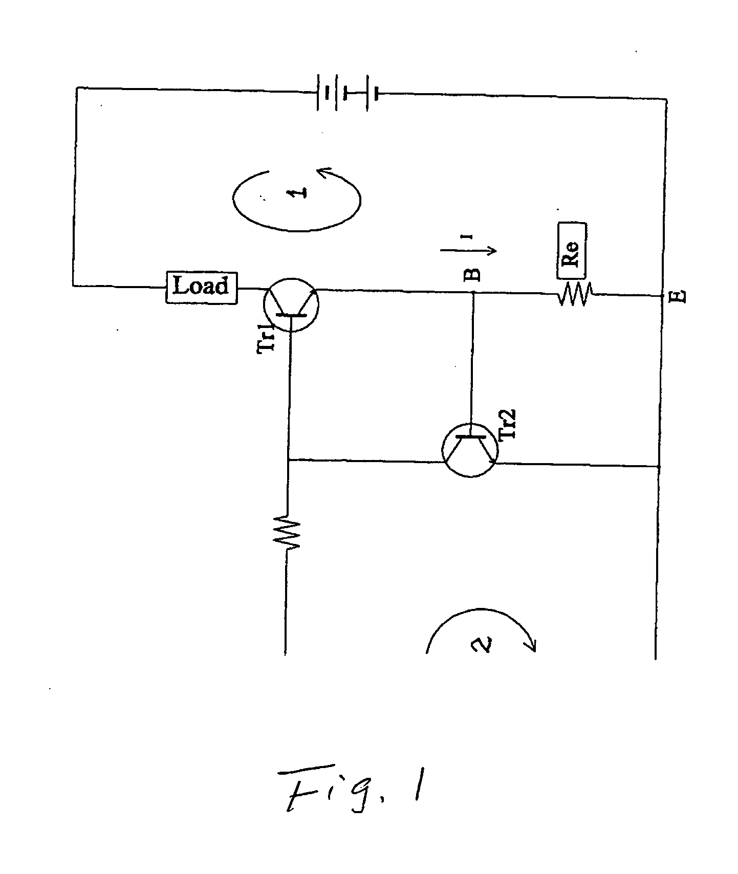
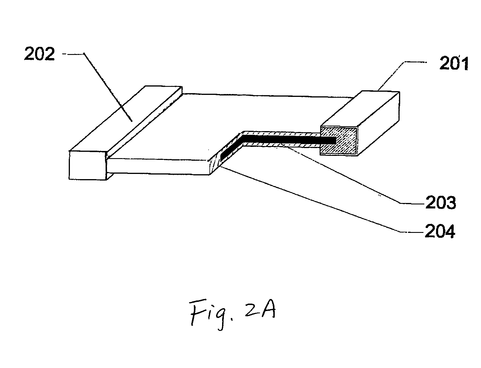
[0025] Referring to FIG. 3 for a current detector of this invention. The current detector includes a detector body 1 and terminals 2 disposed on either sides of the body 1. The detector body is formed as a multiple-layer structure includes a middle substrate layer 10. In a preferred embodiment, the substrate layer 10 is formed as an aluminum oxide layer or a metal layer 10. A bottom heat dissipation layer 11 is attached on the bottom surface of the substrate 10 and a top heat dissipation layer 12 is attached on the top surface of the substrate 10. These heat dissipation layers 11 and 12 composed of FRP epoxy or other attachment agents with high heat conductivity. A resistive layer 13 is formed on top of the top heat dissipation layer 12 and the resistive layer 13 is covered with a protective layer 15. A heat dissipation layer 14, which preferable is a cooper layer is formed below the bottom heat dissipation layer 11 and the heat dissipation layer 14 is covered and protected by a bot...


PUM


Abstract

This invention discloses a current detector formed on a multiple-layered structure with a resistor supported thereon. The multiple-layered structure further includes a heat dissipation layer for dissipating heat generated from the resistor. In a preferred embodiment, the current detector further includes conductive blocks formed by a microelectronic casting process for functioning as part of electrodes for the current detector. In another preferred embodiment, the current detector further includes wrapping around electrodes each with a side conductive surface wrapping around a side surface of the multiple-layered structure.

Description

[0001] This Formal Application claims a Priority Date of Aug. 13, 2003 benefit from a Provisional Patent Applications 60 / 601,673 filed by the same Applicant of this Application respectively. The Provisional Application 60 / 601,673 is hereby incorporated by reference.BACKGROUND OF THE INVENTION [0002] 1. Field of the Invention [0003] This invention relates generally to the device configuration and processes for manufacturing a current detector. More particularly, this invention relates to an improved configuration and process for manufacturing a micro low voltage and low resistance current detector. [0004] 2. Description of the Prior Art [0005] For those of ordinary skill in the art, the configurations and the process of manufacturing a high current inductor coil are still faced with technical challenges that inductor coils manufactured with current technology still does not provide sufficient compact form factor often required by application in modern electronic devices. Furthermore,...

Claims


Application Information

Patent Timeline
IPC IPC(8): H02H5/04
CPCG01R19/32G01R19/0092
Inventor WANG, CHUNG HSIUNG
Owner CYNTEC
Features
  • Generate Ideas
  • Intellectual Property
  • Life Sciences
  • Materials
  • Tech Scout
  • Unparalleled Data Quality
  • Higher Quality Content
  • 60% Fewer Hallucinations
Learn More