Silicon cleaning method for semiconductor materials and polycrystalline silicon chunk

a cleaning method and silicon technology, applied in the direction of polycrystalline material growth, crystal growth process, polycrystalline material growth, etc., can solve the problems of not discussing the action of removing specific metal ions, increasing the requirements for reducing impurities, and increasing so as to reduce the concentration of silicon impurities, significantly reduce specific metal ions, and reduce the effect of impurity concentration

Active Publication Date: 2006-03-02
MITSUBISHI POLYCRYSTALLINE SILICON AMERICA MIPSA +1
View PDF95 Cites 34 Cited by
  • Summary
  • Abstract
  • Description
  • Claims
  • Application Information

AI Technical Summary

Benefits of technology

[0008] The present invention provides a pure water cleaning method that can satisfy such requirements for reducing impurity concentrations of silicon for semiconductor materials. The inventor of the present invention found that removal effects with respect to certain types of metal ions are extremely improved by using pure water that has been purified by combining reverse osmosis treatment and ion exchange treatment during pure water cleaning of polycrystalline silicon chunk used as single crystal silicon raw materials in particular. The present invention is based on the aforementioned finding, and provides an excellent pure water cleaning method capable of significantly reducing specific metal ions.

Problems solved by technology

In the field of semiconductors, increasingly severe quality requirements are being placed on the raw material single crystal silicon accompanying the increasing levels of integration degree.
Particularly, requirements for reducing impurities are becoming extremely severe.
However, an action of removing specific metal ions is not at all discussed in the prior art of the water purifying apparatus.

Method used


Image

  • Silicon cleaning method for semiconductor materials and polycrystalline silicon chunk
  • Silicon cleaning method for semiconductor materials and polycrystalline silicon chunk

Examples


example 1

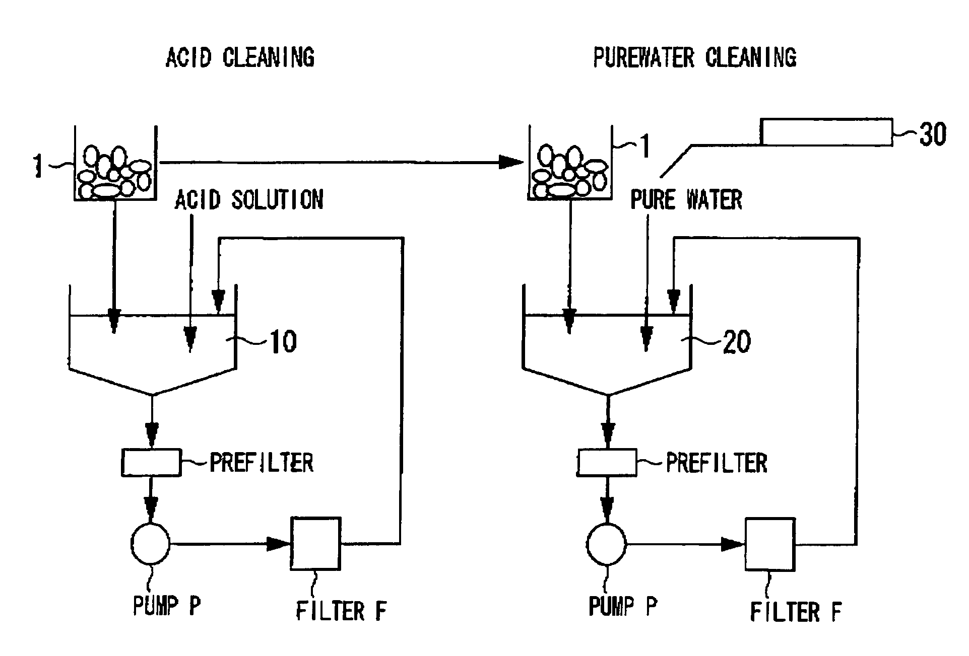
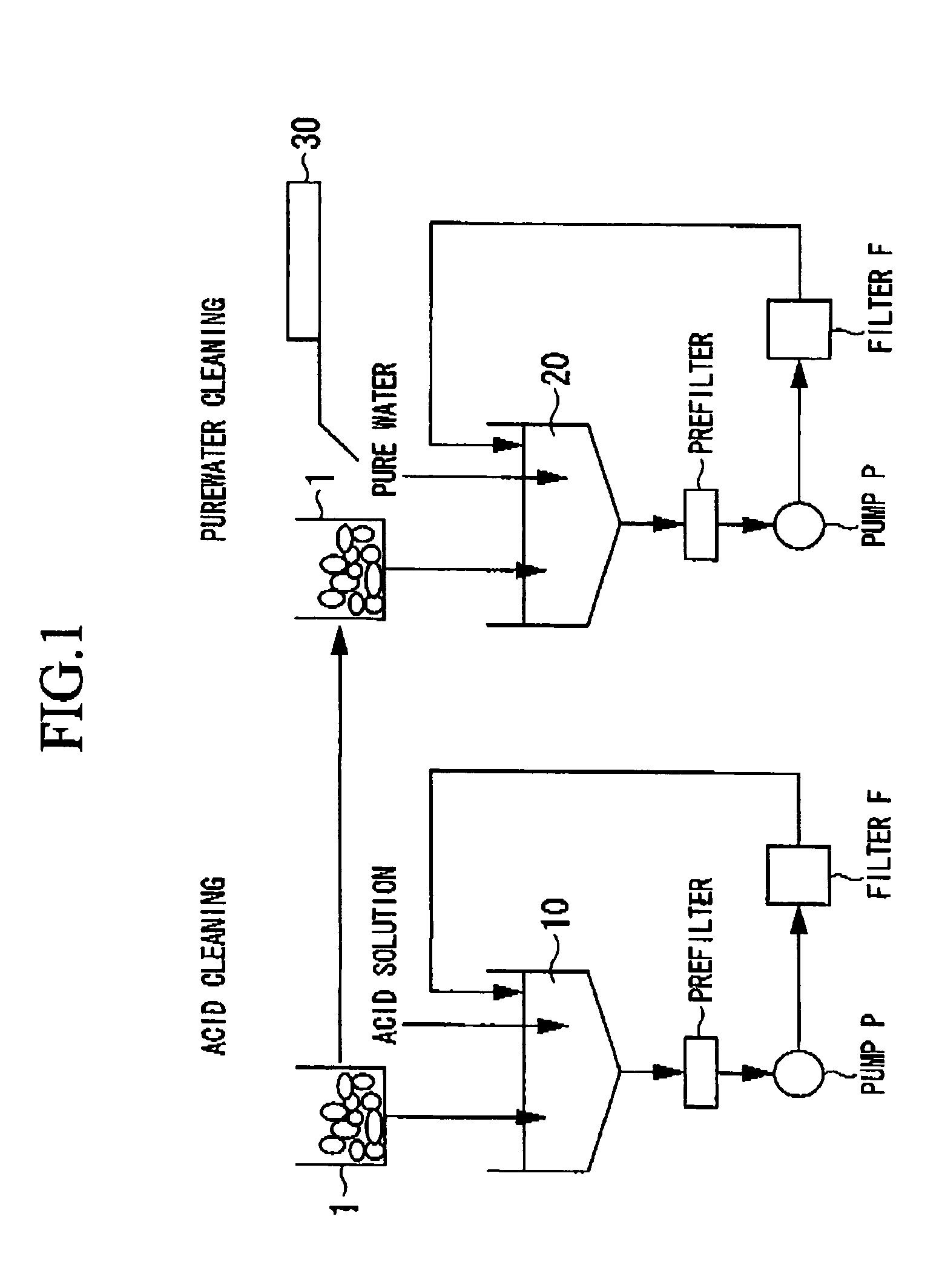
[0041] The cleaning method of the present invention was applied to a pure water rinsing process following an acid cleaning process for a polycrystalline silicon chunk. The acid cleaning process and pure water cleaning process are performed continuously as shown in FIG. 1. As shown in the drawing, a circulation path is provided to each of cleaning tanks 10 and 20 so that, after waste cleaning water is extracted from the bottom of each tank and treated with a filter, water is returned to each of the cleaning tanks. A pre-filter, pump and filter are intermediately provided in the aforementioned circulation paths. While still housed in polyethylene basket 1, the polycrystalline silicon chunk is cleaned by moving from acid cleaning tank 10 to pure water rinsing tank 20 at predetermined immersion times. Furthermore, acid cleaning tank 10 and / or pure water rinsing tank 20 may be formed by multiple tanks.

[0042] A mixed liquid of hydrofluoric acid and nitric acid (70 wt % nitric acid: 50 wt...

example 2

[0045] An 8-inch silicon single crystal was pulled by the CZ method using the polycrystalline silicon shown in Example 1 of Table 1. 150 kg of polyarystalline silicon were charged per one pulling. Pulling was conducted 10 times under the same conditions. The average dislocation free ratio thereof was 98%. On the other hand, when silicon single crystal was pulled under the same conditions using the polycrystalline silicon shown in the comparative example 1 of Table 1, the average dislocation free ratio thereof was 85%.


PUM

PropertyMeasurementUnit
temperatureaaaaaaaaaa
concentrationaaaaaaaaaa

Abstract

A cleaning method cleans silicon for semiconductor materials using pure water treated by a reverse osmosis treatment and by ion exchange treatment and reduces the aluminum and iron remaining on the silicon surface.

Description

BACKGROUND OF THE INVENTION [0001] 1. Field of the Invention [0002] The present invention relates to a silicon cleaning method for semiconductor materials, to a polycrystalline silicon chunk and to a silicon cleaning device. [0003] 2. Description of the Related Art [0004] The single crystal silicon wafers used for semiconductors are produced by melting high-purity polycrystalline silicon (referred to as polysilicon) as a raw material, pulling the single crystal silicon from the molten polysilicon by a method commonly referred to as the CZ method (Czochralski method) and processing this into wafers. The polycrystalline silicon serving as the raw material of the single crystal silicon is mainly obtained in the form of rod-shaped ingots by a CVD reaction in a water-cooled bell jar which is commonly referred to as the Siemens method. These polycrystalline silicon ingots are sent to a single crystal pulling process after going through various processes consisting of cutting, crushing, cl...

Claims


Application Information

Patent Timeline
Patent Type & Authority Applications(United States)
IPC IPC(8): C30B15/00C30B21/06C30B27/02C30B30/04C30B28/10
CPCC30B29/06C30B15/00
Inventor OHTA, HIROTAKE
Owner MITSUBISHI POLYCRYSTALLINE SILICON AMERICA MIPSA
Why Eureka
Try Eureka