Electronic device with a warped spring connector

a technology of electronic devices and connectors, applied in the direction of coupling device connections, semiconductor/solid-state device details, instruments, etc., can solve the problems of cross talk and electrical-magnetic interference between needle electrodes b>120/b>, not all the outer connections are reliable after long hours of operation, signal disconnections, etc., to achieve enhanced reliability of electronic devices 200, prevent metal oxidation and metal contamination, and more flexibility for stress absorption or buffering

Inactive Publication Date: 2006-03-02
CHIPMOS TECH INC
View PDF2 Cites 30 Cited by
  • Summary
  • Abstract
  • Description
  • Claims
  • Application Information

AI Technical Summary

Benefits of technology

[0012] Please refer to FIG. 2 and FIG. 3, the warped spring connectors 220 are disposed on the surface 211 of the substrate 210 and each has a connection end 221 and a suspending end 222. The connection ends 221 are connected to the substrate 210, and the suspending ends 222 are suspended away from the surface 211 of the substrate 210. Each warped spring connector 220 includes a ground lead 223, a dielectric layer 224, and a transmitting lead 225. The dielectric layers 224 are sandwiched between the ground leads 223 and the transmitting leads 225 for electrical isolation. The ground leads 223 can be made from nickel, gold, copper, tungsten, or palladium. The ground leads 223 at the connecting ends 221 are electrically connected to the ground plane 213 of the substrate 210 through the vias 214. The dielectric layers 224 are formed on the corresponding ground leads 223. Preferably, the dielectric layers 224 at the connection ends 221 are connected with the dielectric film over the substrate 210, wherein the dielectric film may be a passivation layer of a wafer, a solder mask or a cover layer of a printed circuit board. Moreover, the dielectric layers 224 are made by PI, BCB, or other flexible dielectric materials. Please refer to FIG. 3. the width of the dielectric layers 224 is larger than the width of the transmitting leads 225 to electrically isolate the transmitting leads 225 and the ground leads 223. The transmitting leads 225 are formed on the dielectric layers 224 and are bonded to the signal bonding pads 212 of the substrate 210. The transmitting leads 225 can contain a metal chosen from the group consisting of nickel, gold, copper, tungsten, or palladium. The thickness of the transmitting leads 225 is larger than the thickness of the ground leads 223, and the CTE of the transmitting leads 225 is smaller than the CTE of the dielectric layer 224 or / and the CTE of the ground leads 223. For example, the transmitting leads 225 are made of Invar, Kovar with a very low CTE. Therefore, an internal thermal stress inside the warped spring connectors 220 is created such that the suspending ends 222 move further away from the substrate 210 as operation temperature increases. It is to provide more flexibility for stress absorption or buffering, i.e., the reliability of the electronic device 200 is enhanced. Preferably, each warped spring connector 220 further includes an anti-wetting metal layer 226, such as palladium (Pd), which covers each transmitting lead 225 to prevent metal oxidation and metal contamination from the bonding pads. The thickness of the anti-wetting metal layers 226 in the range of several hundred Å to several micrometers (μm) is much smaller than the thickness of the transmitting leads 225 in the range of 10 to 100 μm.
[0013] The ground leads 223 act as ground shielding for the corresponding transmitting leads 225. Therefore, the signal transmission between the transmitting leads 225 will not be interfered by other transmitting leads 225 nor the circuits inside the substrate 210 nor the EMI from a printed circuit board. The crosstalk and noise can be well isolated or eliminated by means of the warped spring connectors 220. The structure of the warped spring connectors 220 is most suitable for longer and thinner electrical connections with better stress absorption capability for smaller pitches and higher density high speed, high frequency applications.
[0014] As shown in FIG. 2, the warped spring connectors 220 are fabricated by electroplating, sputtering, or deposition in the sequence of the ground leads 223, the dielectric layers 224, and the transmitting leads 225. During the fabrication processes, a sacrificial layer (not shown in the figure), such as photoresist or etchable metal, is formed between the ground leads 223 and the substrate 210 except the connecting ends 221, and then the ground leads 223 are formed on the sacrificial layer on the surface 211 of the substrate 220. Accordingly, the ground leads 223 can be easily released and separated from the surface 211 of the substrate 210 after finishing the dielectric layers 224 and the transmitting leads 225. Then due to the CTE mismatch between the transmitting leads 225 and the dielectric layers 224 or between the transmitting leads 225 and the ground leads 223, the suspending ends 222 of the warped spring connectors 220 can be released in the air and suspended away from the surface 211 of the substrate 210. Preferably, a recess 215 is formed in the surface 211 of the substrate 220 for formation of the sacrificial layer to easily separate the ground leads 223 from the substrate 210.

Problems solved by technology

However, not all the outer connections are reliable after long hours of operation due to mismatch of the coefficients of thermal expansion (CTE) between the electronic devices and printed circuit boards connected by the outer connections.
Any breakdown between outer connections and printed circuit boards will cause electrically open which leading to signal disconnections, i.e., system failure.
However, when higher density of electrical connections or smaller line widths and pitches are required, the cross talk and electrical-magnetic interferences between needle electrodes 120 will become severe.
The needle electrodes cannot be implemented in high speed, high frequency applications.

Method used


Image

  • Electronic device with a warped spring connector
  • Electronic device with a warped spring connector
  • Electronic device with a warped spring connector

Examples


Embodiment Construction

[0010] Please refer to the attached drawings, the present invention will be described by means of an embodiment below.

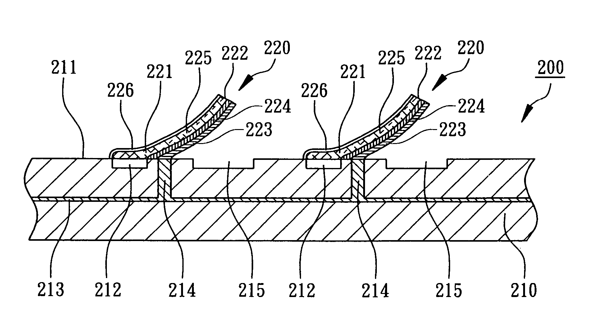
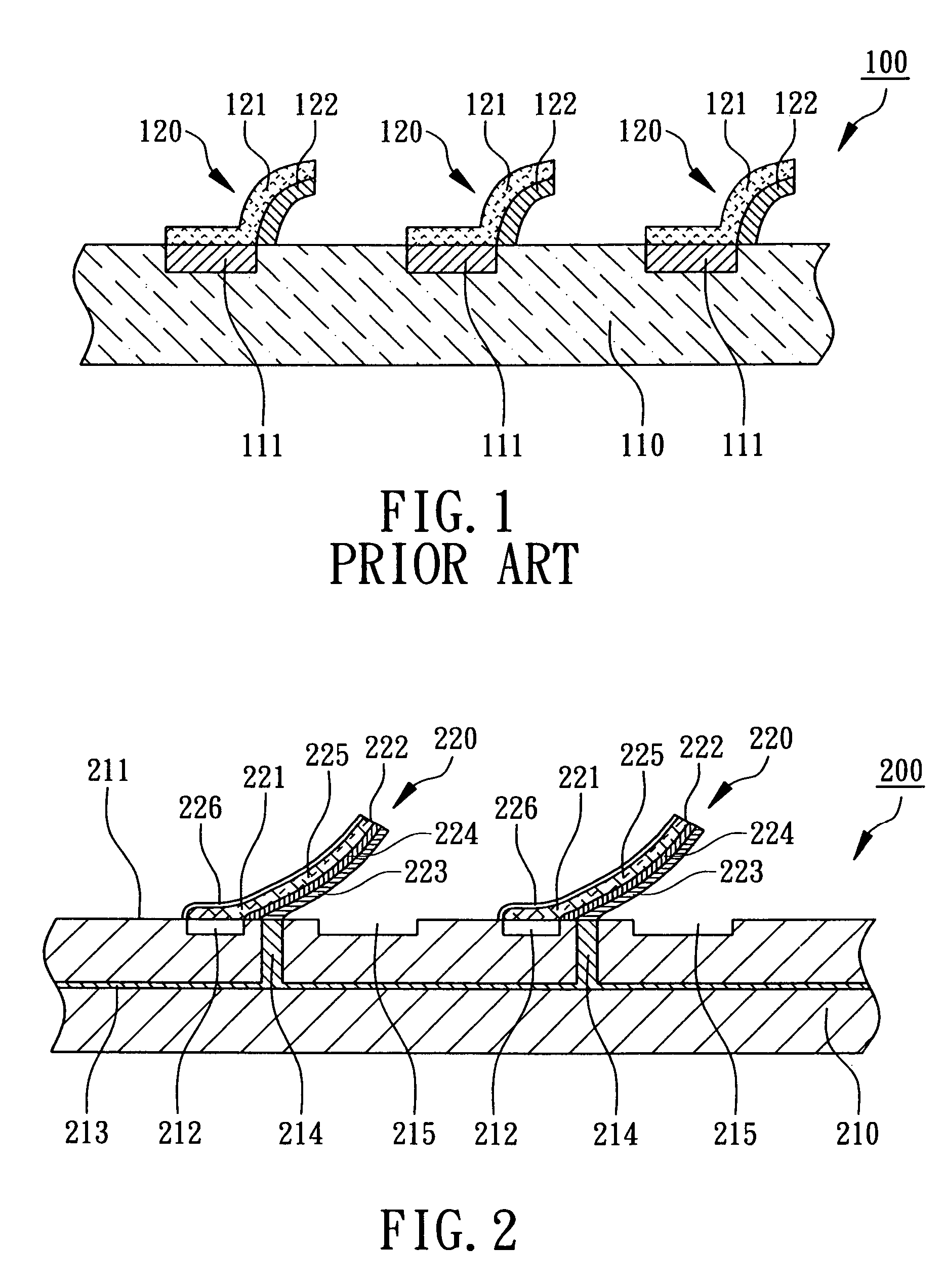
[0011] Referring to FIG. 2, an electronic device according to a preferred embodiment of the present invention is described. The electronic device 200 comprises a substrate 210 and a plurality of warped spring connectors 220. The substrate 210 has a plurality of signal bonding pads 212 on its surface 211, a ground plane 213 in the substrate 210, and a plurality of vias 214. The substrate 210 is chosen from the group consisting of wafer, chip, wafer-level chip scale package (WLCSP), silicon substrate, ceramic substrate, glass substrate, and printed circuit board. The surface 211 may be an active surface with integrated circuits (IC) or a probing surface of a probe head of a probe card so that the electronic device 200 can be implemented in IC packaging as well as in IC testing.

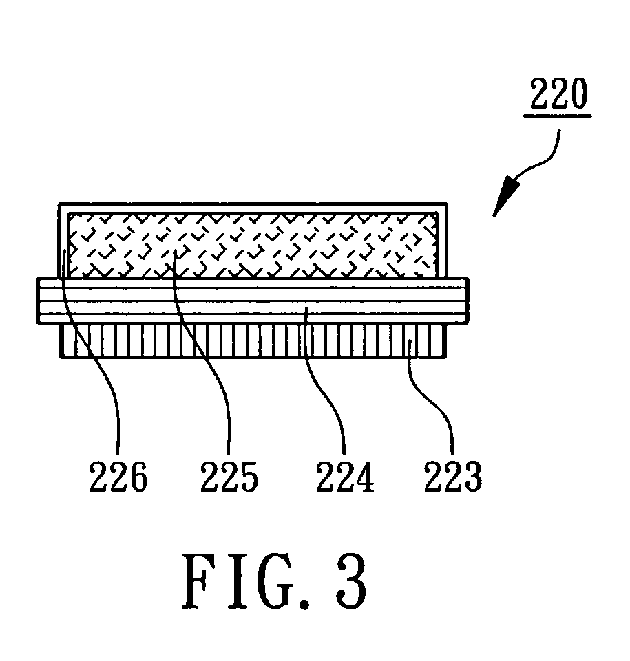
[0012] Please refer to FIG. 2 and FIG. 3, the warped spring connectors 220 are disposed on ...


PUM


Abstract

An electronic device comprises a substrate and at least a warped spring connector. The substrate has a signal bonding pad and a ground plane. The warped spring connector is disposed on the substrate and is connected to the bonding pad. The warped spring connector includes at least a ground lead electrically connected to the ground plane, a dielectric layer on the ground lead, and a transmitting lead on the dielectric layer. The transmitting lead is bonded to the bonding pad. The ground lead is isolated from and close to the transmitting lead to solve cross-talk and noise problem. Furthermore, the coefficient of thermal expansion of the transmitting lead is different from that of the dielectric layer or the ground lead such that the warped spring connector has a suspending end suspending away from the substrate.

Description

FIELD OF THE INVENTION [0001] The present invention relates to an electronic device, and more particularly to an electronic device with a warped spring connector. BACKGROUND OF THE INVENTION [0002] There are various outer connections for electronic devices such as bumps, solder balls, bonding wires, probes, gold fingers, leads, etc. However, not all the outer connections are reliable after long hours of operation due to mismatch of the coefficients of thermal expansion (CTE) between the electronic devices and printed circuit boards connected by the outer connections. The capability of stress absorbing or buffering of the outer connections under larger temperature gradients becomes the key factor for ensuring good reliability. Any breakdown between outer connections and printed circuit boards will cause electrically open which leading to signal disconnections, i.e., system failure. [0003] According to Taiwan Patent Publication Number 535,226 submitted by the applicants, entitled “an ...

Claims


Application Information

Patent Timeline
Patent Type & Authority Applications(United States)
IPC IPC(8): H01R12/04H05K1/09G01R1/067H01L21/28
CPCH01L24/72H01L2924/01029H01L2924/01046H01L2924/01074H01L2924/01079H01L2924/01082G01R1/06727H01L2924/14H01L2924/3025H01R13/2407H05K1/0216H05K3/4092H01L2924/01033H01L2924/09701H01L2924/351H01L2924/15787H01L2924/00
Inventor LEE, YI-CHANGLIU, AN-HONGWANG, YEONG-HERCHAO, YEONG-CHINGLEE, YAO-JUNG
Owner CHIPMOS TECH INC
Why Eureka
Try Eureka