Stacked photoelectric converter

a technology of photoelectric converter and stacked photoelectric converter, which is applied in the direction of photovoltaics, electrical devices, semiconductor devices, etc., can solve the problems of increasing the production cost and time, increasing the apparatus cost, and reducing the properties of the photoelectric conversion module, so as to reduce production costs and time, increase the current generated by the front photoelectric conversion unit, and high dark conductivity

Active Publication Date: 2006-03-02
KANEKA CORP
View PDF8 Cites 81 Cited by
  • Summary
  • Abstract
  • Description
  • Claims
  • Application Information

AI Technical Summary

Benefits of technology

[0043] In the stacked-layer type photoelectric conversion device according to the present invention, the incident light is partially reflected at the interface between the silicon composite layer and the semiconductor layer contacting the same. This can increase the current generated by the front photoelectric conversion unit. Alternatively, the photoelectric conversion layer in the front photoelectric conversion unit can be made thinner to generate the same current as in the case that the silicon composite layer is not provided.
[0044] Since the silicon composite layer can be formed by plasma CVD similarly as in the case of the photoelectric conversion unit, the front photoelectric conversion unit, the silicon composite layer and the back photoelectric conversion unit can all be formed in the similar plasma CVD apparatus. This elimina

Problems solved by technology

As described above, when a TCO layer of ZnO or the like is used as the intermediate reflective layer in the stacked-layer type photoelectric conversion device, the method of forming the TCO layer differs from that for semiconductor layers, and thus an apparatus or a film deposition chamber for forming the TCO layer should be additionally provided, which inevitably increases the apparatus costs.
Further, in the case that the integrated type thin-film photoelectric conversion module is formed including the TCO layer as the intermediate reflective layer, the leakage current possibly occurs in the structure having the first and second is

Method used


Image

  • Stacked photoelectric converter
  • Stacked photoelectric converter
  • Stacked photoelectric converter

Examples


example 2

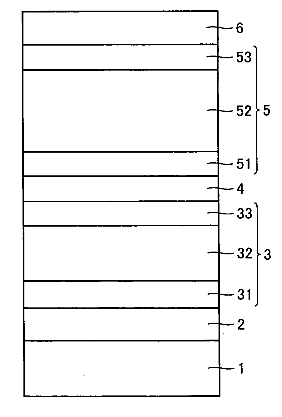
[0137] A stacked-layer type photoelectric conversion device as shown in FIG. 17 was fabricated as Example 2. The device of Example 2 differs from the device of Example 1 of FIG. 10 only in that a 30 nm thick n-type silicon composite layer 4 is employed as the n-type layer of front photoelectric conversion unit 3 to serve both as the intermediate reflective layer and the n-type layer.

[0138] As seen from Table 1, in Example 2 compared to Example 1, Jsc is further increased and Eff is further improved, and the spectral sensitivity currents of both the front and back photoelectric conversion units are increased, presumably for the following reason. Since silicon composite layer 4 also serves as the n-type layer of front photoelectric conversion unit 3, light reflected to the front photoelectric conversion unit 3 side and light transmitted to the back photoelectric conversion unit 5 side are both unnecessary to transmit the 30 nm thick n-type microcrystalline silicon layer, resulting in...

example 3

[0141] A stacked-layer type photoelectric conversion device as shown in FIG. 18 was fabricated as Example 3. The device of Example 3 differs from the device of Example 2 of FIG. 17 only in that the n-type layer of front photoelectric conversion unit 3 is formed by stacking a 30 nm thick n-type silicon composite layer 34 as a first n-type layer and a 5 nm thick n-type microcrystalline silicon layer 35 as a second n-type layer. Needless to say, the n-type silicon composite layer 34 of Example 3 is formed under plasma CVD conditions similar to those for n-type silicon composite layer 4 in Examples 1 and 2.

[0142] As seen from Table 1, although Jsc in Example 3 is slightly decreased compared to Example 2, FF and Eff are improved. Further, although the spectral sensitivity current of the front photoelectric conversion unit in Example 3 is slightly lower than that of Example 2, it is higher than those of Comparative Example 1 and Example 1. This is presumably because insertion of n-type m...

example 4

[0143] A stacked-layer type photoelectric conversion device as shown in FIG. 19 was fabricated as Example 4. The device of Example 4 differs from the device of Example 2 of FIG. 17 only in that the n-type layer of front photoelectric conversion unit 3 is formed by stacking a 10 nm thick n-type microcrystalline silicon layer 36 as a first n-type layer, a 60 nm thick n-type silicon composite layer 37 as a second n-type layer and a 5 nm thick n-type microcrystalline silicon layer 38 as a third n-type layer.

[0144] As seen from Table 1, although Jsc in Example 4 is slightly decreased compared to Example 3, FF and Eff are improved. This is presumably because n-type microcrystalline silicon layer 36 inserted between i-type amorphous silicon layer 32 and n-type silicon composite layer 37 has decreased the contact resistance at the i / n interface, and thus FF is further improved compared to Example 3. In Example 4, n-type microcrystalline silicon layer 36 and n-type microcrystalline silicon ...


PUM


Abstract

In a stacked-layer type photoelectric conversion device, a plurality of photoelectric conversion units are stacked on a substrate, each of which includes a one conductivity-type layer, a photoelectric conversion layer of substantially intrinsic semiconductor and an opposite conductivity-type layer in this order from a light-incident side. At least one of the opposite conductivity-type layer in a front photoelectric conversion unit arranged relatively closer to the light-incident side and the one conductivity-type layer in a back photoelectric conversion unit arranged adjacent to the front photoelectric conversion unit includes a silicon composite layer at least in a part thereof. The silicon composite layer has a thickness of more than 20 nm and less than 130 nm and an oxygen concentration of more than 25 atomic % and less than 60 atomic %, and includes silicon-rich phase parts in an amorphous alloy phase of silicon and oxygen.

Description

TECHNICAL FIELD [0001] The present invention relates to improvement of conversion efficiency of a thin-film photoelectric conversion device, and more particularly to improvement of conversion efficiency of a stacked-layer type thin-film photoelectric conversion device having a plurality of photoelectric conversion units stacked one another. Herein, the terms “crystalline” and “microcrystalline” are used also for denoting a solid state partially including amorphous parts, as generally used in the art. BACKGROUND ART [0002] In recent years, to simultaneously achieve lower costs and higher efficiency of a photoelectric conversion device, thin-film photoelectric conversion devices having almost no problem from the standpoint of resources have attracted attention, and development thereof has been tried vigorously. Application of the thin-film photoelectric conversion devices to various uses such as solar batteries, optical sensors, displays and others have been expected. An amorphous sil...

Claims


Application Information

Patent Timeline
IPC IPC(8): H01L31/105H01L31/052H01L31/076H01L31/077
CPCH01L31/076H01L31/077H01L31/056Y02E10/548Y02E10/52Y02E10/547H01L31/00
Inventor SASAKI, TOSHIAKIKOI, YOHEIYAMAMOTO, KENJIYOSHIMI, MASASHIICHIKAWA, MITSURU
Owner KANEKA CORP
Why Eureka
Try Eureka