Isolation techniques for reducing dark current in CMOS image sensors

a technology of image sensor and isolation technology, which is applied in the direction of semiconductor devices, radio frequency controlled devices, electrical equipment, etc., can solve the problems of affecting and reducing the detection accuracy of cmos image sensors

Active Publication Date: 2006-03-02
MICRON TECH INC
View PDF19 Cites 21 Cited by
  • Summary
  • Abstract
  • Description
  • Claims
  • Application Information

AI Technical Summary

Benefits of technology

[0013] These and other features and advantages of the invention will be more apparent from the following detailed description that is provided in connection with the accompanying drawings and illustrate exemplary embodiments of the invention.

Problems solved by technology

One drawback associated with shallow trench isolation in the case of CMOS image sensors is cross-talk from a photon impinging on a particular pixel of a photosensitive device causing changes that may diffuse under the shallow trench isolation structure to an adjacent pixel.
Another drawback is that a hole accumulation layer along the sidewall of the trench is relatively small since it is limited by the depth of the shallow trenches.
One technique which may be used to improve pixel isolation in CMOS image sensors is to implant dopants beneath the isolation region; however, it has been found that this may contribute undesirably to pixel dark current.

Method used


Image

  • Isolation techniques for reducing dark current in CMOS image sensors
  • Isolation techniques for reducing dark current in CMOS image sensors
  • Isolation techniques for reducing dark current in CMOS image sensors

Examples


first embodiment

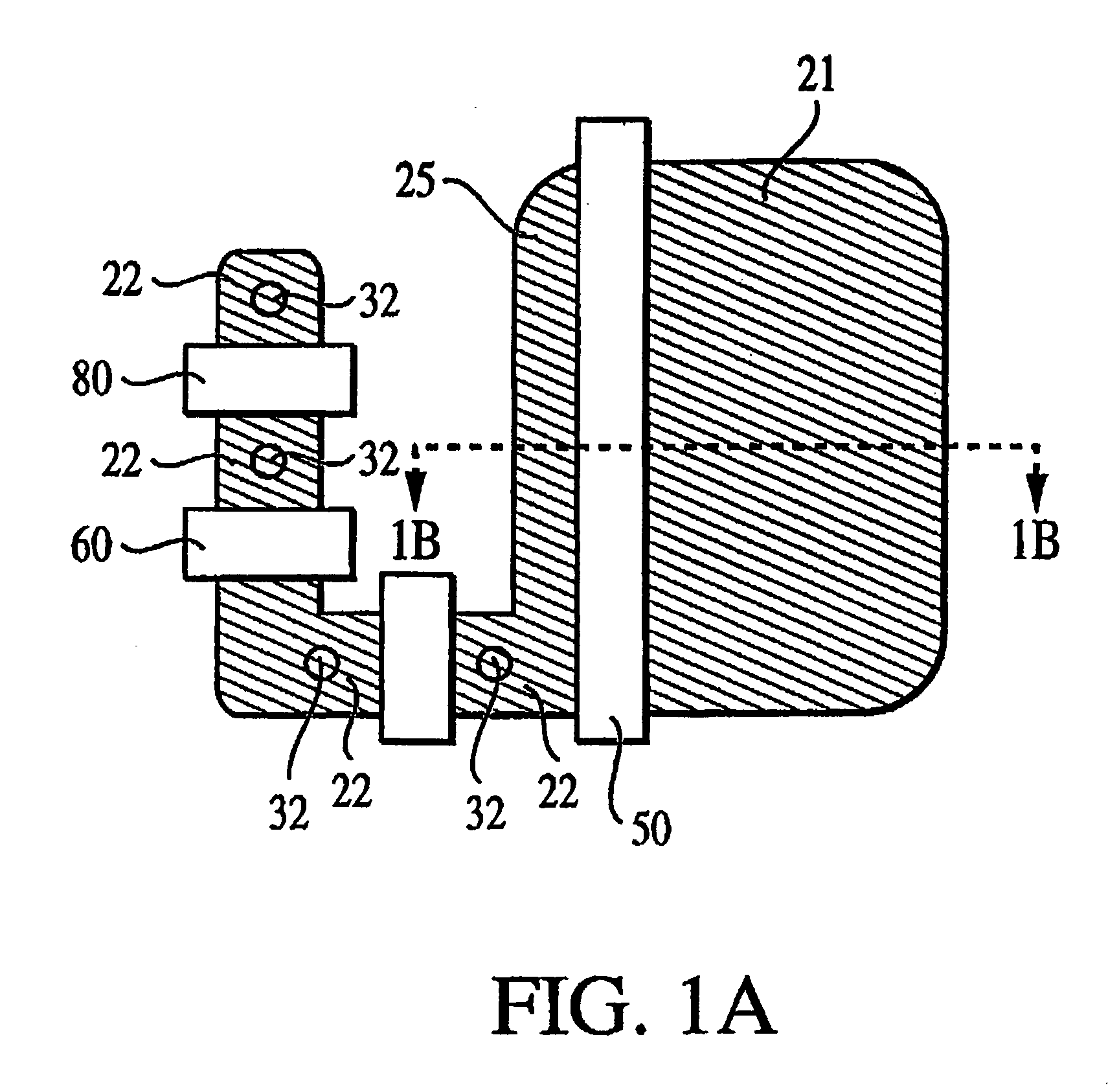
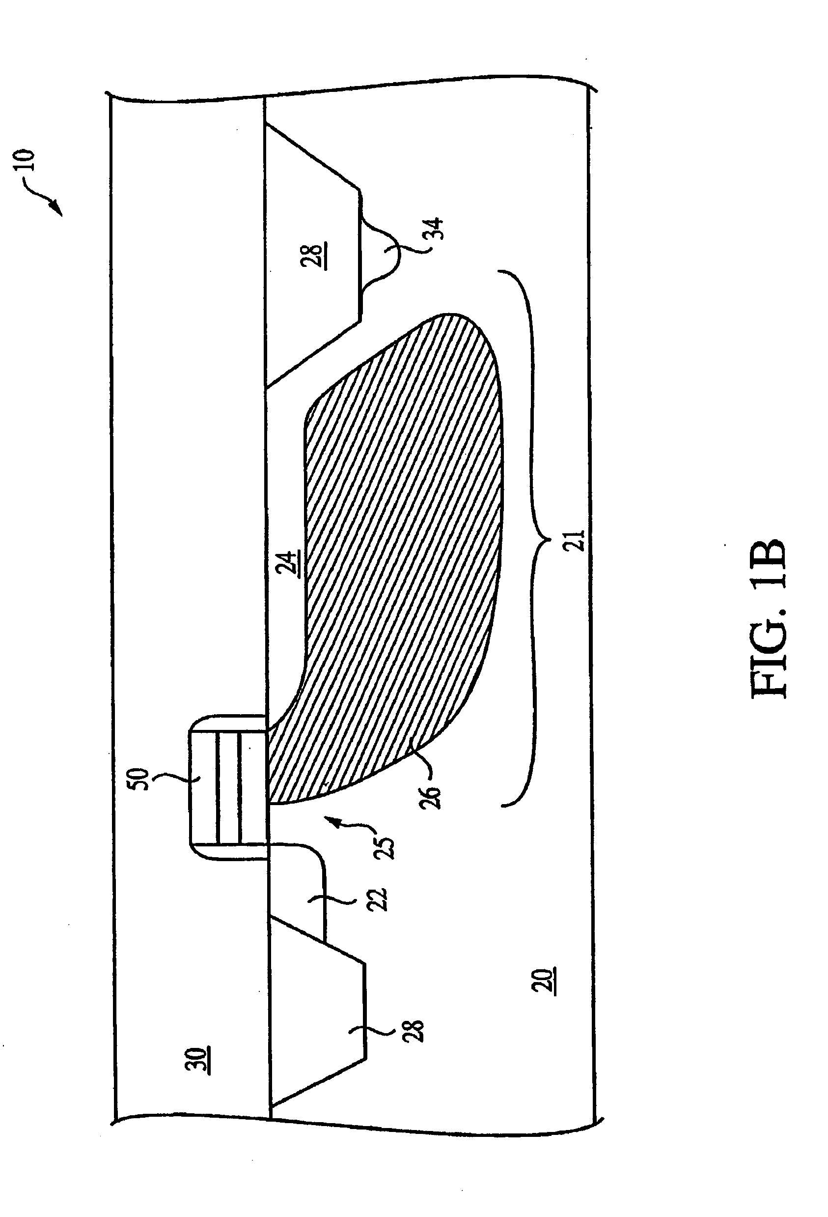
[0041] A first embodiment according to the invention is now described with reference to FIGS. 2-6. Applicant proposes an STI process, which uses an isolation trench filled with a doped conductive material containing silicon. Shallow trench isolation regions for CMOS image sensors generally have a depth of less than about 3000 Angstroms and generally around about 2000 to about 2500 Angstroms. Typically, shallow trench regions are filled with a conventional insulator, such as oxides or high density plasma (HDP) oxides. However, it is difficult to fill trenches having a depth greater than 2500 Angstroms with conventional insulators due to the limited spacing within the trench, for example, undesirable voids or air gaps are formed when oxides are used to fill trenches having a depth greater than about 2500 Angstroms. In accordance with the invention, Applicant proposes filling trenches with conductive materials containing silicon, preferably polysilicon or silicon-germanium. Conductive ...

second embodiment

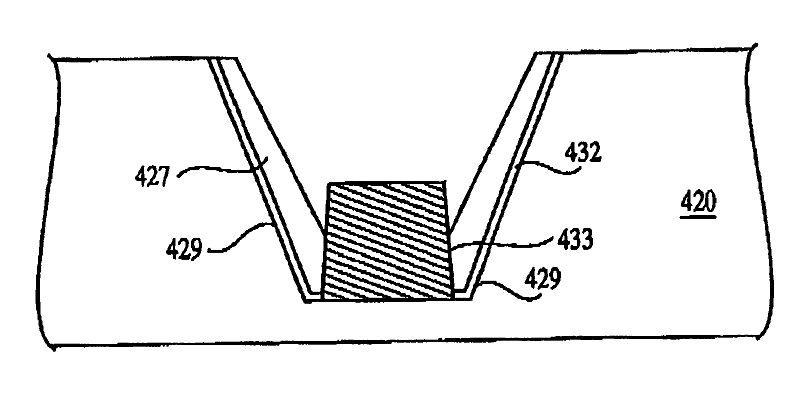
[0051] A second embodiment in accordance with the invention is now described with reference to FIGS. 7-13. Referring now to FIG. 7, a trench 428 is etched into an active layer 420. The trench is preferably a deep trench having a depth greater than about 2500 Angstroms and preferably between about 4000 to about 5000 Angstroms. A resist and mask are applied, and photolithographic techniques are used to define the area to be etched-out. A directional etching process, such as RIE, or etching with a preferential anisotropic etchant is used to etch into the doped active layer 420 to form the trench 428. The resist and mask are removed leaving the FIG. 7 structure.

[0052] Referring now to FIG. 8, a nitride liner 432 is formed in the trench 428 via Chemical Vapor Deposition (CVD). This nitride liner 432 may be formed of any suitable nitride including NO, ON, ONO, and is preferably formed of silicon nitride.

[0053] Referring now to FIG. 9, an oxide, e.g. SiO2 or other dielectric liner 427 is ...


PUM


Abstract

A structure for isolating areas in a semiconductor device is provided. The structure includes a trench having first and second portions formed in a substrate. The first portion has a first width, and the second portion has a second width and is below the first portion. The first width is greater than the second width. A first insulating liner is formed along at least lateral sidewalls of the first portion. A spacer material is formed along at least lateral sidewalls of the insulating liner and filling the second portion. A filler material is over said spacer material and within the first portion. Methods for forming the structure are also provided.

Description

CROSS REFERENCE TO RELATED APPLICATIONS [0001] The present application is a continuation-in-part of U.S. application Ser. No. 10 / 291,772, filed on Nov. 12, 2002, now U.S. Pat. No. 6,888,214, issued May 3, 2005, the disclosure of which is herewith incorporated by reference in its entirety.FIELD OF THE INVENTION [0002] The present invention relates generally to semiconductor devices, and more particularly, to trench isolation technology for use in semiconductor devices, including CMOS image sensors. BACKGROUND OF THE INVENTION [0003] In silicon integrated circuit (IC) fabrication, it is often necessary to isolate semiconductor devices formed in the substrate. This is true for many semiconductor memory devices, for example, DRAM, flash memory, SRAM, microprocessors, DSP and ASIC. The individual pixels of a CMOS image sensor also need to be isolated from each other. [0004] A CMOS image sensor circuit includes a focal plane array of pixel cells, each one of the cells includes a photogate...

Claims


Application Information

Patent Timeline
Patent Type & Authority Applications(United States)
IPC IPC(8): H01L29/00
CPCH01L27/1463H01L27/14689H01L27/14687
Inventor MOULI, CHANDRA
Owner MICRON TECH INC
Why Eureka
Try Eureka