
Method and apparatus for providing a modulation current

a modulation current and modulation method technology, applied in pulse generators, semiconductor lasers, pulse techniques, etc., can solve the problems of increasing error rates, speed limitations in regulation, and difficulty in achieving high output impedances, and achieve the effect of improving modulation

Active Publication Date: 2006-03-02
IBM CORP
View PDF3 Cites 13 Cited by
  • Summary
  • Abstract
  • Description
  • Claims
  • Application Information

AI Technical Summary

Benefits of technology

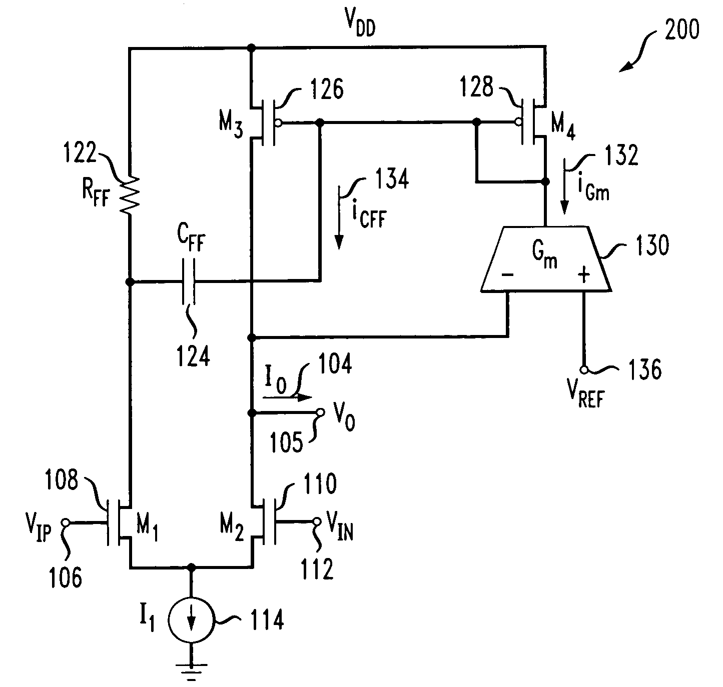
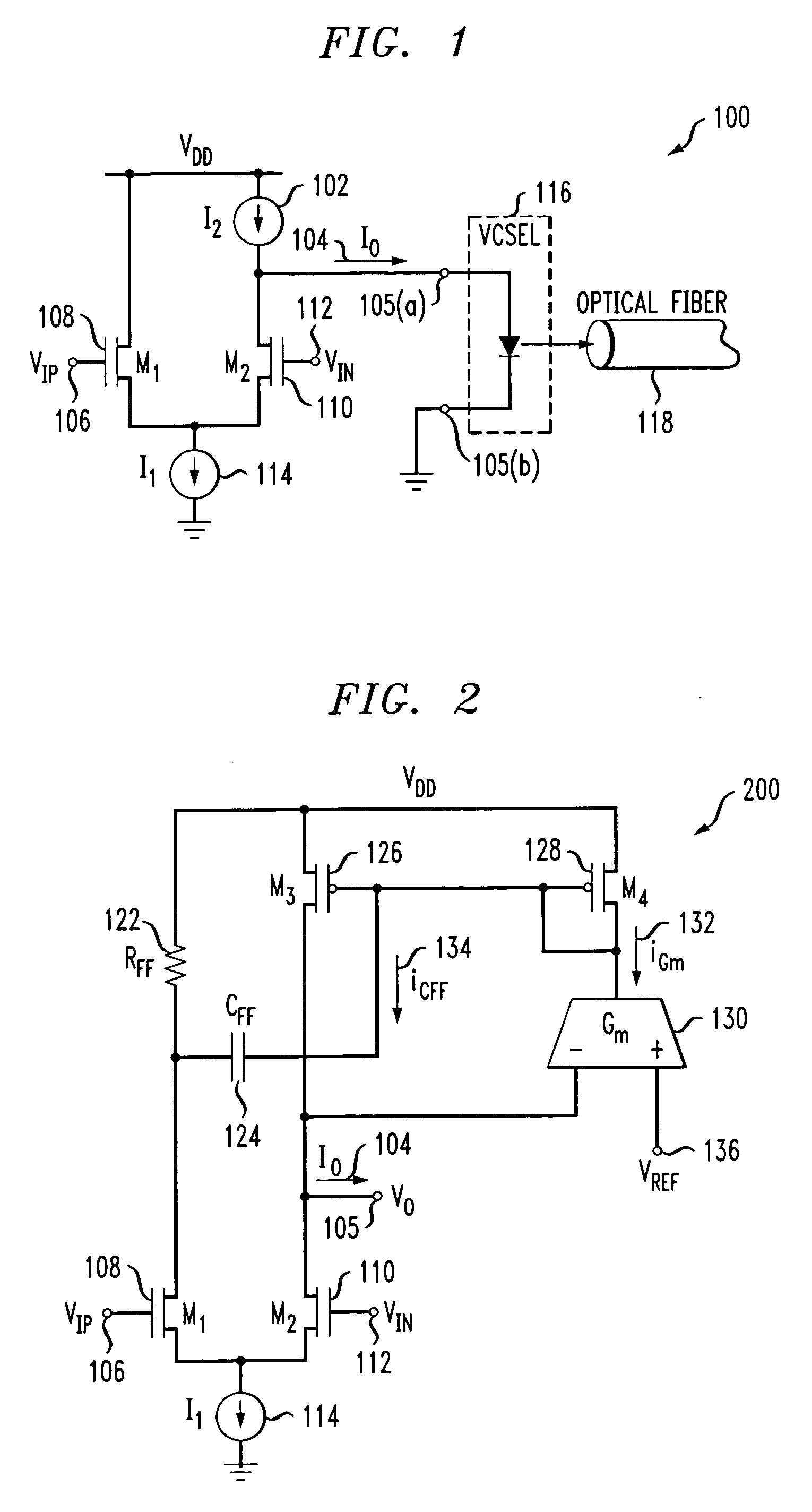
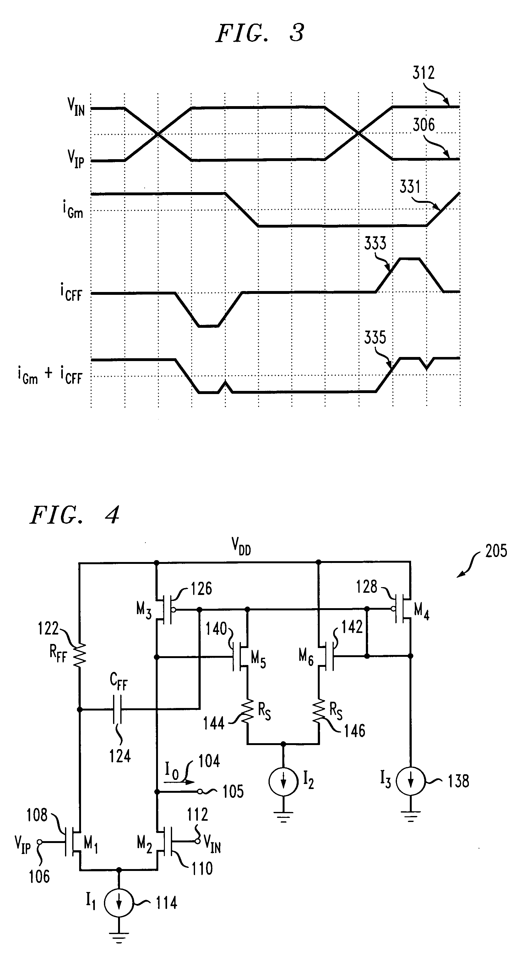
The present invention provides improved techniques for generating modulation currents. One aspect involves generating a control signal for a current source based on an input voltage difference and modulating the output current. The control node of the current source is preconditioned and the modulation current is provided to a load as a function of the current through the current source. Another aspect involves shaping the modulation current waveform by generating a signal to shape the waveform and providing it to the output node via a variable tail current of a modulating circuit. This involves combining feed-forward and pre-distortion aspects. Overall, the invention provides more efficient and effective techniques for generating modulation currents.

Problems solved by technology

In the latter case, advances in CMOS (complementary metal-oxide-semiconductor) technologies make achieving high output impedances more difficult because of the short-channel effects in transistors, such as channel length modulation.
Alternatively, active impedance regulation may be used, but such regulation has speed limitations due to the feedback control loop.
However, operating lasers near their maximum frequencies causes a variety of non-ideal transient behaviors that can cause inter-symbol interference (ISI), which unfortunately increases the error rate.

Method used


Image

  • Method and apparatus for providing a modulation current
  • Method and apparatus for providing a modulation current
  • Method and apparatus for providing a modulation current

Examples


Embodiment Construction

[0027] When designing MOSFET (metal oxide semiconductor field effect transistor) devices, it is advantageous to design them with minimum channel lengths, since this minimizes parasitic capacitance for a given bias current. However, short channel MOSFET devices are more susceptible to channel length modulation, a short-channel effect that can significantly reduce drain-to-source impedance of a MOSFET device in the saturation state, causing a single short-channel MOSFET to be a less-than ideal current source. This characteristic also affects most of the advanced BiCMOS (bipolar complementary metal oxide semiconductor) technologies including SiGe (silicon germanium). These characteristics are mitigated, in accordance with principles of the invention, by generating a modulation current via techniques that include output impedance compensation with feed-forward bandwidth enhancement.

[0028]FIG. 1 shows a schematic diagram of a transconductance amplifier (TCA)-type laser diode driver (LDD...


PUM


Abstract

Techniques are disclosed for providing modulation current that includes output impedance compensation with a feed-forward bandwidth enhancement and pre-distortion modulation to control waveform transition symmetry. A feedback circuit senses output node voltage and increases the overdrive voltage of a current source. This offsets the loss of current due to channel length modulation and increases the effective output impedance of the source. A feed-forward circuit enhances the bandwidth of the impedance compensation feedback loop. Waveform transition symmetry is improved by pre-distorting a laser modulation current by introducing an undershoot current on the falling edge of the modulating current.

Description

FIELD OF THE INVENTION [0001] This invention relates generally to a method and apparatus for providing a modulation current and, more particularly, this invention relates to providing a modulation current that is a function of feedback, feed-forward bandwidth enhancement and / or waveform shaping. BACKGROUND OF THE INVENTION [0002] High speed semiconductor applications require accurate control over output impedance of a circuit. Voltage outputs typically require an output impedance that is matched to an electrical transmission line and a load that the circuit is driving. Current outputs typically require a high output impedance to consistently operate with a variety of loads. In the latter case, advances in CMOS (complementary metal-oxide-semiconductor) technologies make achieving high output impedances more difficult because of the short-channel effects in transistors, such as channel length modulation. In CMOS technology, transistors are used to realize logic functions, and in high ...

Claims


Application Information

Patent Timeline
Patent Type & Authority Applications(United States)
IPC IPC(8): H03C1/00
CPCH01S5/042
Inventor KUCHARSKI, DANIEL
Owner IBM CORP
Learn More