Package substrate for a semiconductor device, a fabrication method for same, and a semiconductor device

a technology for semiconductor devices and packaging substrates, which is applied in the direction of fixed capacitors, dielectric characteristics, fixed capacitor details, etc., can solve the problems of high fabrication cost, inconvenient multi-layer construction of core materials, and inefficient and impractical methods, etc., to facilitate multiple-layer configuration, facilitate fabrication, and facilitate the effect of electrical connection reliability

Active Publication Date: 2006-03-02
DENSO CORP +1
View PDF25 Cites 46 Cited by
  • Summary
  • Abstract
  • Description
  • Claims
  • Application Information

AI Technical Summary

Benefits of technology

[0024] It is an object of the present invention to provide a package substrate for a semiconductor device that is easy to fabricate, that, compared to the prior art, facilitates a multiple layer configuration, and that has higher reliability of electrical connections, to provide a fabrication method of such a semiconductor device package substrate, and to provide a semiconductor device that includes this semiconductor device package substrate.

Problems solved by technology

The built-up multilayer board such as disclosed in the example of Japanese Patent Application Laid-Open No. 2004-158671 involves the formation of core material 101 followed by the successive formation of a plurality of substrate layers 102 and therefore necessitates an extremely time-consuming fabrication process and high fabrication costs.
For example, this method is inefficient and impractical when fabricating a multilayer board having ten or more layers, and in particular, thirteen or more layers.
However, the adoption of core material 101 having a multilayer construction is not preferable due to the further increase in fabrication time and fabrication costs.
In addition, the incorporation of glass cloth in core material 101 raises the concern that penetration by moisture might lead to the occurrence of dendrites.
This requirement interferes with the high-density wiring and prevents an adequate response to the demand for a more compact semiconductor device package.
In addition, because core material 101 is thick, the formation of vias by embedding metal in through-holes becomes problematic due to the difficulty of the fabrication steps and the amount of metal material that must be used.
This construction therefore suffers from the problem of poor freedom degree of design.
In addition, when flip-chip integrated circuit elements 109 are mounted on one of the outermost layers of this multilayer board and a motherboard (not shown) is connected to the outermost layer on the opposite side, the reliability of the connection between integrated circuit elements 109 and the multilayer board is poor.
On the other hand, a ceramic multilayer board such as was disclosed in Japanese Patent Application Laid-Open No. 2002-118194 does not allow green sheets of very thin construction.
For example, when constructing a multilayer board having ten or more, or in particular, having thirteen or more layers, the thickness of the green sheets, which each have a thickness of, for example, 2 mm or more, complicates their use as a package for semiconductor devices.
However, the final dimensional accuracy of conductive pattern 106 is poor in this fabrication method, and adequate control of the position of conductive pattern 106 to obtain the desired impedance is therefore extremely difficult.
In addition, when flip-chip integrated circuit elements 109 are mounted on one outermost layer of this multilayer board and a motherboard (not shown) is connected to the outermost layer on the opposite side, the reliability of the package connections are poor.
This poor reliability results from the great difference between the linear expansion coefficient of the ceramic that is the main material of the multilayer board (4-6 ppm in the direction of thickness and 4-6 ppm in the surface direction) and the linear expansion coefficient of the glass epoxy resin that is the main material of the motherboard (16-17 ppm in the direction of thickness and 60 ppm in the surface direction).
In addition, the semiconductor device package is subject to a high degree of stress.
Further, the dielectric constant of a ceramic is higher than that of an organic material, and the loss of the high-frequency signal that passes through the conductive pattern is therefore great.

Method used


Image

  • Package substrate for a semiconductor device, a fabrication method for same, and a semiconductor device
  • Package substrate for a semiconductor device, a fabrication method for same, and a semiconductor device
  • Package substrate for a semiconductor device, a fabrication method for same, and a semiconductor device

Examples


Embodiment Construction

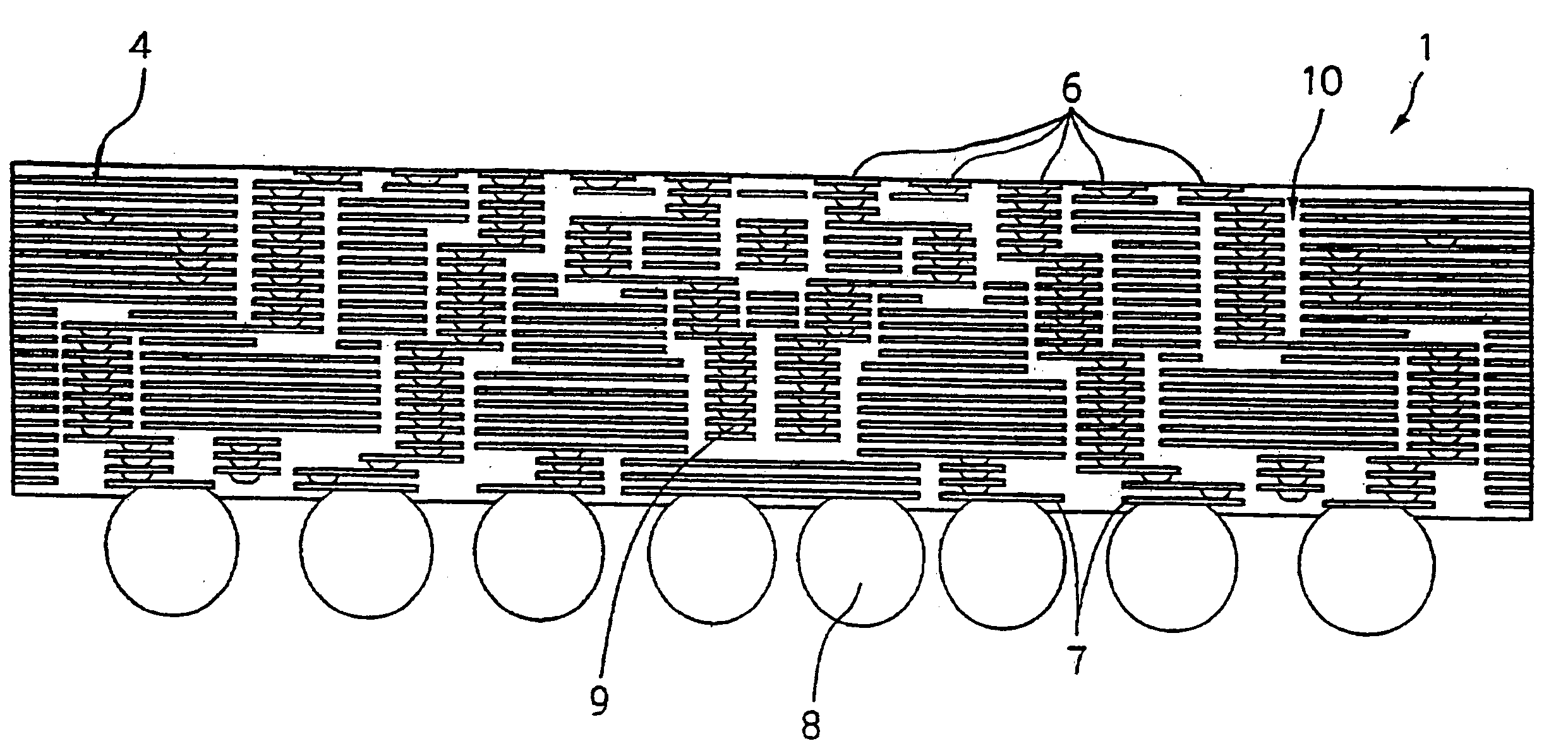
[0079]FIG. 7 shows the semiconductor device of the present invention, and FIG. 8 shows a package substrate (multilayer board) 1 for this semiconductor device. The following explanation first regards the basic configuration of this semiconductor device. In this semiconductor device, an integrated circuit element of the flip-chip connection type such as LSI chip 2 is mounted on one outermost layer of multilayer board 1. A motherboard 3, which is an external board, is connected on the outermost layer of the opposite side of multilayer board 1. Multilayer board 1 is a super-multilayer board having 23 layers of conductive patterns 4. A plurality of connection terminals 6 for securing connection bumps 5 of LSI chip 2 is exposed to the outside on one outermost layer. A multiplicity of metal pads 7 is provided on the outermost layer of the opposite side and ball terminal (solder ball) 8 is secured on each metal pad 7 to form a ball grid array (BGA) construction for connecting with motherboa...


PUM

PropertyMeasurementUnit
radiusaaaaaaaaaa
thicknessaaaaaaaaaa
weight %aaaaaaaaaa

Abstract

A plurality of film insulators having conductive patterns that are formed on surfaces and conductive vias that pass through the film insulators in the direction of thickness are stacked together and collectively subjected to pressure and heat to be formed as a single unit. On one outermost layer of the multilayer board that has been thus formed, a plurality of connection terminals are exposed to the outside, connection bumps of an LSI chip being secured to these connection terminals. On the outermost layer of the opposite side, a multiplicity of metal pads are provided, and a solder ball is secured on each metal pad to form a ball grid array (BGA) structure for connecting to a motherboard.

Description

BACKGROUND OF THE INVENTION [0001] 1. Field of the Invention [0002] The present invention relates to a package substrate for a semiconductor device in which integrated circuit elements are mounted, to a method of fabricating the package substrate, and to a semiconductor device that includes the package substrate for a semiconductor device. [0003] 2. Description of the Related Art [0004] Packages are conventionally used for incorporating integrated circuit elements such as LSI chips and connecting the integrated circuit elements to what is called a “motherboard” (circuit board). Such a package incorporates a multilayer board on which various signal lines, ground patterns, and power-supply patterns have been formed. The integrated circuit elements and motherboard are connected by way of this multilayer board. [0005] Multilayer boards for packaging of the prior art include the built-up type of multilayer board that is disclosed in, for example, Japanese Patent Application Laid-Open No....

Claims


Application Information

Patent Timeline
Patent Type & Authority Applications(United States)
IPC IPC(8): H05K1/00
CPCH05K2201/09781H05K2201/2009H01L2924/01327H05K2203/1178H01L23/49816H01L23/49827H01L2224/16H01L2924/01078H01L2924/01079H01L2924/15311H01L2924/3011H01L2924/3025H05K1/0271H05K1/114H05K3/4617H05K3/4632H05K2201/0129H05K2201/0394H05K2201/068H05K2201/09063H05K2201/096H01L2224/16225H01L2924/01019H01L2924/00H01L2924/00014H01L2924/00011H01L2224/0401H01L23/12H01L23/52
Inventor HAYASHI, AKIMORISUZUKI, KATSUNOBUOIKAWA, RYUICHINAKAGOSHI, MAKOTOSERA, NAOKOMURAI, TADASHIOGIHARA, CHIHOKATAOKA, RYOHEIKONDO, KOJIYOKOCHI, TOMOHIRO
Owner DENSO CORP
Why Eureka
Try Eureka