Repair of carbon depletion in low-k dielectric films

Inactive Publication Date: 2006-03-02
INFINEON TECH AG
View PDF15 Cites 25 Cited by
  • Summary
  • Abstract
  • Description
  • Claims
  • Application Information

AI Technical Summary

Benefits of technology

[0017] In yet other embodiments, derivatization reactions may fabricate rather than repair low-k, dielectric films. For example, porous sil

Problems solved by technology

A major drawback with low-k dielectrics is that they are susceptible to damage from plasma etching and ashing processes used in device fabrication.
In etch and ash processing, low-k materials frequently suffer from carbon depletion at the surface exposed to the plasmas.
In certain etch and ash processes, the damage may also extend into the bulk as well.
It is also known that the damaged low-k dielectric material is vulnerable to chemical attack during exposure to wet chemical cleanups, which results in significant critical dimension (CD) loss of low-k dielectric film insulating structures.
However, thermal annealing raises concerns regard

Method used


Image

  • Repair of carbon depletion in low-k dielectric films
  • Repair of carbon depletion in low-k dielectric films
  • Repair of carbon depletion in low-k dielectric films

Examples


Embodiment Construction

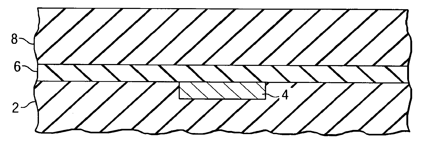
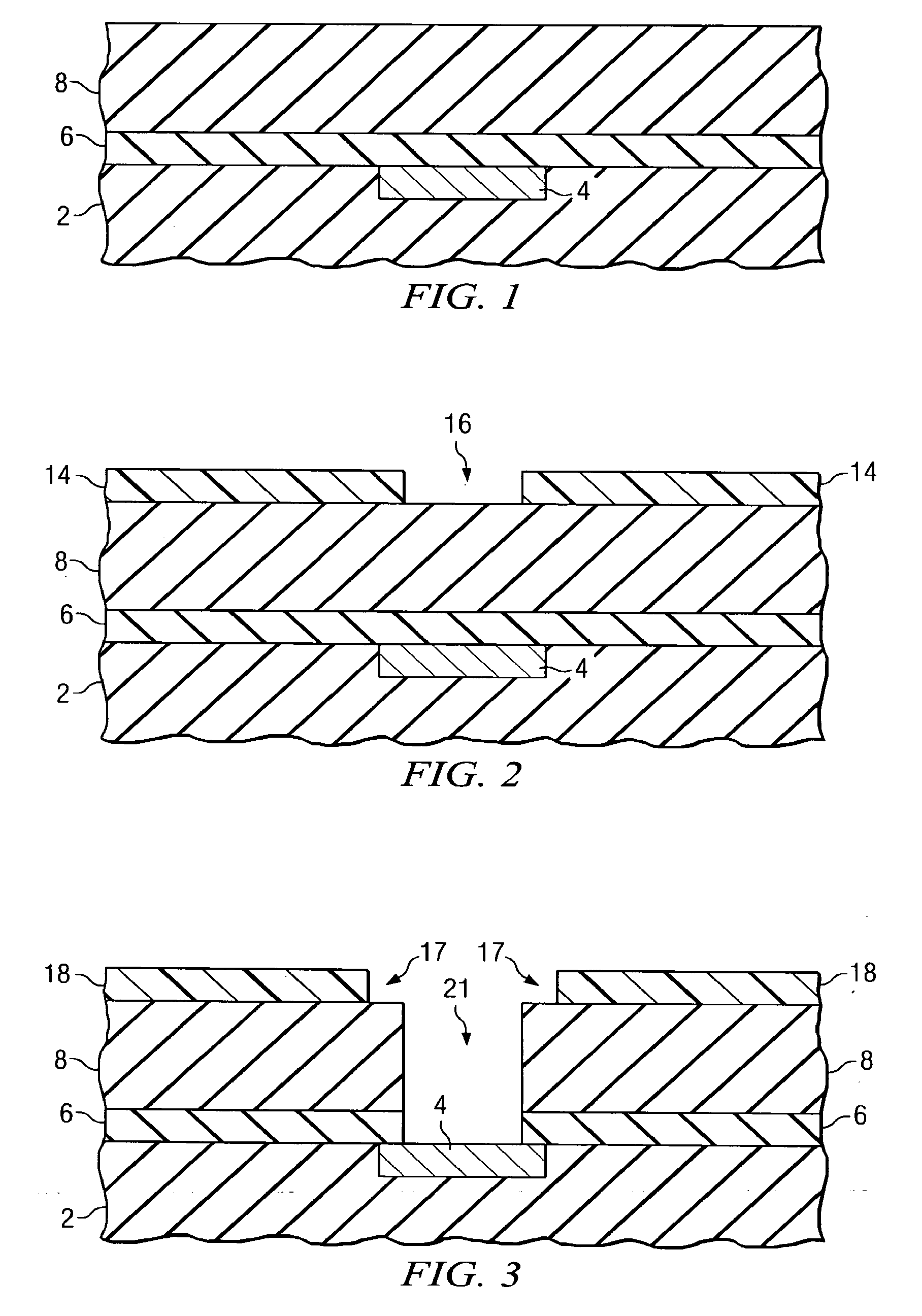
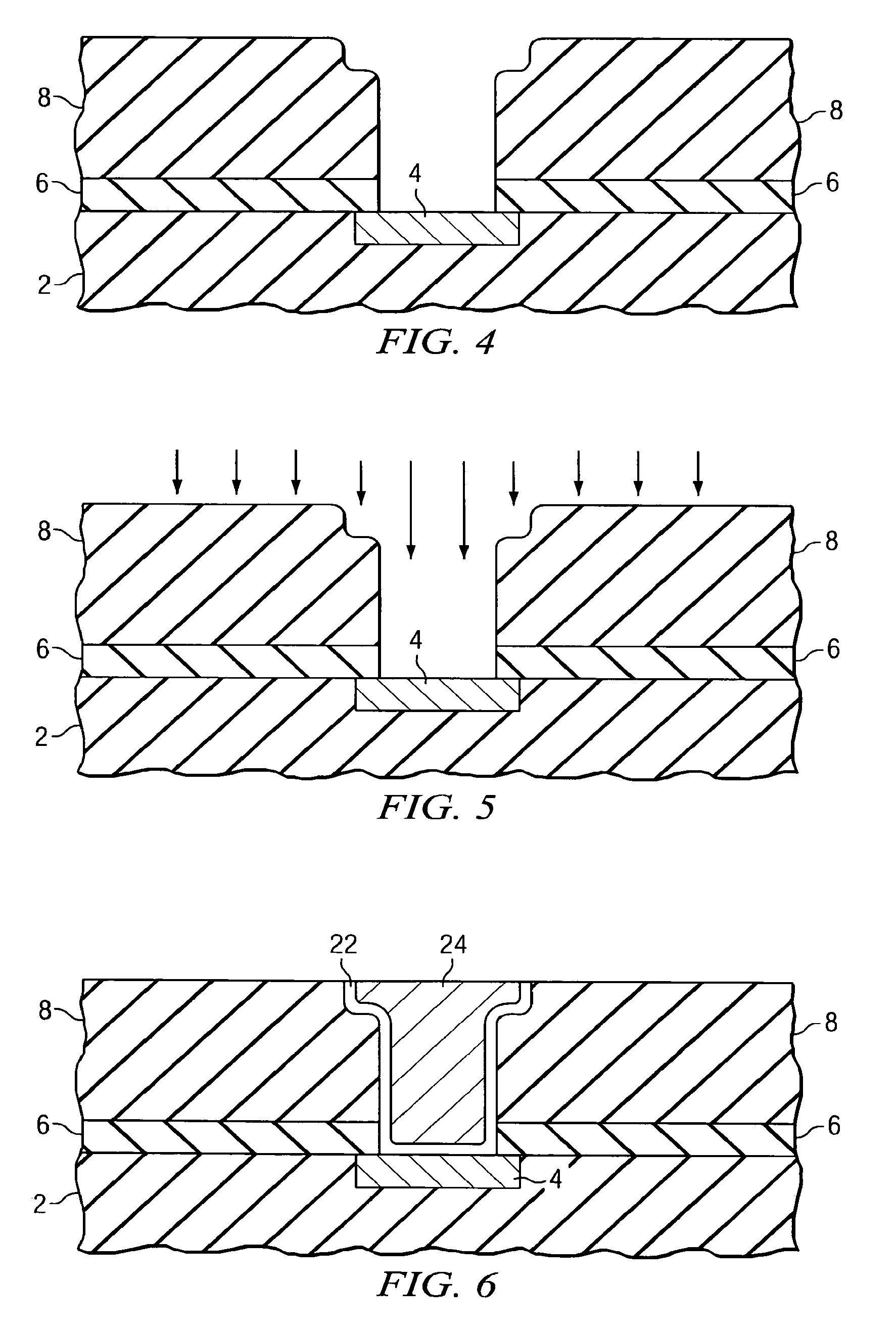
[0022] The making and using of the presently preferred embodiments are discussed in detail below. It should be appreciated, however, that the present invention provides many applicable inventive concepts that may be embodied in a wide variety of specific contexts.

[0023] The present invention will now be described with respect to preferred embodiments in a specific context, namely specific steps in the manufacture an integrated circuit comprising multiple level copper metallization formed by way of a dual damascene process. Complete details of an exemplary dual damascene manufacturing process are provided in U.S. Pat. No. 6,521,542 to Armacost et al. and are incorporated herein by reference. It is believed that embodiments of this invention are advantageous when used in a damascene metallization process. It is further believed that embodiments described herein will benefit other manufacturing stages involving low-k films not specifically illustrated. Therefore, the specific embodime...


PUM


Abstract

A method of repairing damaged low-k dielectric materials is disclosed. Plasma-based processes, which are commonly used in semiconductor device manufacturing, frequently damage carbon-containing, low-k dielectric materials. Upon exposure to moisture, the damaged dielectric material may form silanol groups. In preferred embodiments, a two-step approach converts the silanol to a suitable organic group. The first step includes using a halogenating reagent to convert the silanol to a silicon halide. The second step includes using a derivatization reagent, preferably an organometallic compound, to replace the halide with the suitable organic group. In a preferred embodiment, the halogenating agent includes thionyl chloride and the organometallic compound includes an alkyllithium, preferably methyllithium. In another preferred embodiment, the organometallic compound comprises a Grignard reagent. Embodiments disclosed herein advantageously enable the manufacturer to engineer the density, polarization, and ionization properties of the low-k dielectric material by selective incorporation of the organic group.

Description

TECHNICAL FIELD [0001] This invention relates generally to semiconductor device manufacturing and more particularly to the formation and processing of dielectric films. BACKGROUND [0002] A goal of semiconductor device manufacturing is to make integrated circuits as small as possible. As devices become smaller, low-k dielectrics are needed to reduce parasitic capacitance and RC switching delay. These materials are particularly useful as intermetal dielectrics, or IMDs, and as interlayer dielectrics, or ILDs. [0003] Low-k dielectric materials refer to those insulating materials that have a dielectric constant lower than that of silicon dioxide, or less than about 4. One example of a low-k material is fluorine-doped silicon dioxide, or fluorosilicate glass (FSG). Another widely used material is a carbon-doped oxide or organosilicate glass (OSG). OSG films typically comprise SiwCxOyH, wherein the tetravalent silicon may have a variety of organic group substitutions. A commonly used subs...

Claims


Application Information

Patent Timeline
IPC IPC(8): H01L21/31
CPCH01L21/02126H01L21/02203H01L21/02271H01L21/02304H01L21/02337H01L21/76807H01L21/02362H01L21/3105H01L21/3122H01L21/31633H01L21/02343
Inventor WEBER, FRANK
Owner INFINEON TECH AG
Why Eureka
Try Eureka