Method of forming fluorine-doped low-dielectric-constant insulating film

a technology of low-dielectric constant and film, applied in the field of simiconductor formation technologies, can solve the problems of poor thermal stability of films, and achieve the effect of improving the thermal stability of films deposited with fluorine-doped materials

Active Publication Date: 2006-03-02
ASM JAPAN
View PDF3 Cites 19 Cited by
  • Summary
  • Abstract
  • Description
  • Claims
  • Application Information

AI Technical Summary

Benefits of technology

[0008] The present invention was achieved in view of the above-mentioned problems. Among others, an object of the present invention in an embodiment is to provide a method of forming fluorine-doped low-dielectric-constant silicon oxide films having a low dielectric constant and high thermal stability. Another object of the present invention in an embodiment is to provide a method of forming fluorine-doped low-dielectric-constant silicon oxide films without increasing apparatus costs.
[0010] In the above aspect, when the fluorine-doped silicon oxide film is nearly or substantially free of hydrogen, its thermal stability can improve significantly. The film can be obtained by using the above specific RF power which facilitates dissociation of hydrogen, and by using CO2 at the above specific rate.
[0012] In a preferred embodiment, the processing gas may further comprise an inert gas at a flow rate more than ten times that of SiH4 (e.g., ratios of inert gas / SiH4 of 11 / 1, 13 / 1, 15 / 1, 20 / 1, 30 / 1, and ranges between any two numbers of the foregoing). The inert gas may be He and / or Ar. The inert gas is effective to stabilize plasmas.
[0016] In still another aspect, the present invention provides a method of forming a fluorine-doped silicon oxide film containing less than 1 atomic % of hydrogen and less than 2 atomic % of carbon, using capacitive-coupled plasma CVD. The method comprises: (i) introducing a processing gas comprising SiH4 as a silicon source gas, SiF4 as a fluorine source gas, and CO2 as an oxygen source gas without including O2 gas to a reaction chamber; and (ii) generating an O-containing plasma for oxidizing the SiH4 and the SiF4 to deposite a fluorine-doped silicon oxide film on a substrate while generating a CO-containing plasma for controlling the oxidization, using a combination of a frequency of about 10 MHz to about 30 MHz and a frequency of about 400 kHz to about 500 kHz to dissociate hydrogen nearly or substantially without doping carbon into the fluorine-doped silicon oxide film. Under the above conditions, despite the fact that CO2 is used as an oxygen source gas, carbon is nearly or substantially not doped into the film. Although carbon may be detected in the film, carbon may not be incorporated into the film structure, but may be present as a contaminant. The film is nearly or substantially free of hydrogen, resulting in excellent thermal stability. In this aspect, one or more of any ranges and elements usable in the aforesaid embodiments can be used.
[0018] In yet another aspect, the present invention provides a method of forming a fluorine-doped silicon oxide film containing nearly or substantially no hydrogen and nearly or substantially no carbon doped, using capacitive-coupled plasma CVD. The method comprises: (i) introducing a processing gas comprising SiH4 as a silicon source gas, SiF4 as a fluorine source gas, and CO2 as a single oxygen source gas to a reaction chamber; (ii) applying first RF power at a frequency of about 10 MHz to about 30 MHz and second RF power at a frequency of about 400 kHz to about 500 kHz by overlaying the two RF powers to generate a plasma reaction field within the reaction chamber, thereby depositing on a substrate a fluorine-doped silicon oxide film containing nearly or substantially no hydrogen and nearly or substantially no carbon doped; and (iii) improving thermal stability of the depositing fluorine-doped silicon oxide film as a function of a flow of CO2 with respect to that of the sum of SiH4 and SiF4 and as a function of concentration of hydrogen in the film. In this aspect, one or more of any ranges and elements usable in the aforesaid embodiments can be used.
[0019] The present invention can be applied to a fluorine-doped silicon oxide film obtained by any of the methods described above. The film may preferably contain 30-45 atomic % (e.g., 35 atomic %, 40 atomic %, and ranges between any two numbers of the foregoing) of silicon, 50-70 atomic % (e.g., 55 atomic %, 60 atomic %, 65 atomic %, and ranges between any two numbers of the foregoing) of oxygen, 4-8 atomic % (e.g., 5 atomic %, 6 atomic %, 7 atomic %, and ranges between any two numbers of the foregoing) of fluorine, less than 1 atomic % (e.g., 0.5 atomic %, 0.1 atomic %, and ranges between any two numbers of the foregoing) of hydrogen, less than 2 atomic % (e.g., 1.5 atomic %, 1.0 atomic %, 0.5 atomic %, and ranges between any two numbers of the foregoing) of carbon, and less than 1 atomic % (e.g., no detectable amount) of nitrogen. In a preferred embodiment, the concentration of each element is nearly or substantially constant in a thickness direction. According to one or more methods described above, the concentration of hydrogen does not increase as the film is depositing, i.e., hydrogen does not accumulate during film formation, thereby accomplishing uniformity of properties in a thickness direction.

Problems solved by technology

Additionally, from the result of temperature-programmed desorption (TDS, thermal disorption spectroscopy), desorption of H2O, F, and HF at 400° C. or higher is significant, which indicates that the films' thermal stability is poor.

Method used


Image

  • Method of forming fluorine-doped low-dielectric-constant insulating film
  • Method of forming fluorine-doped low-dielectric-constant insulating film
  • Method of forming fluorine-doped low-dielectric-constant insulating film

Examples


examples

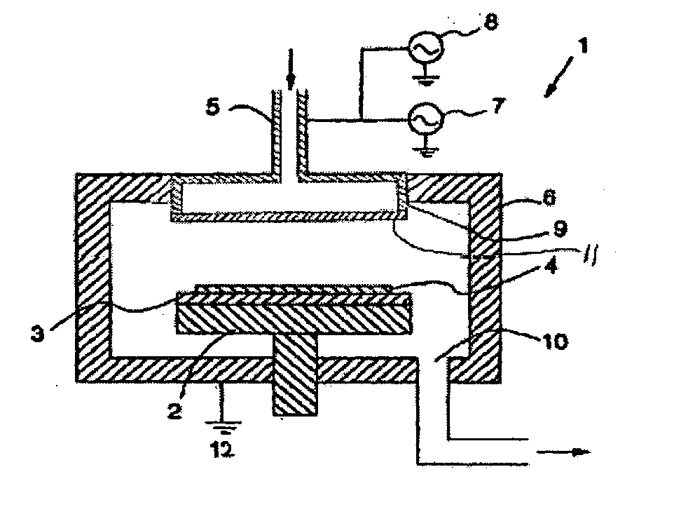
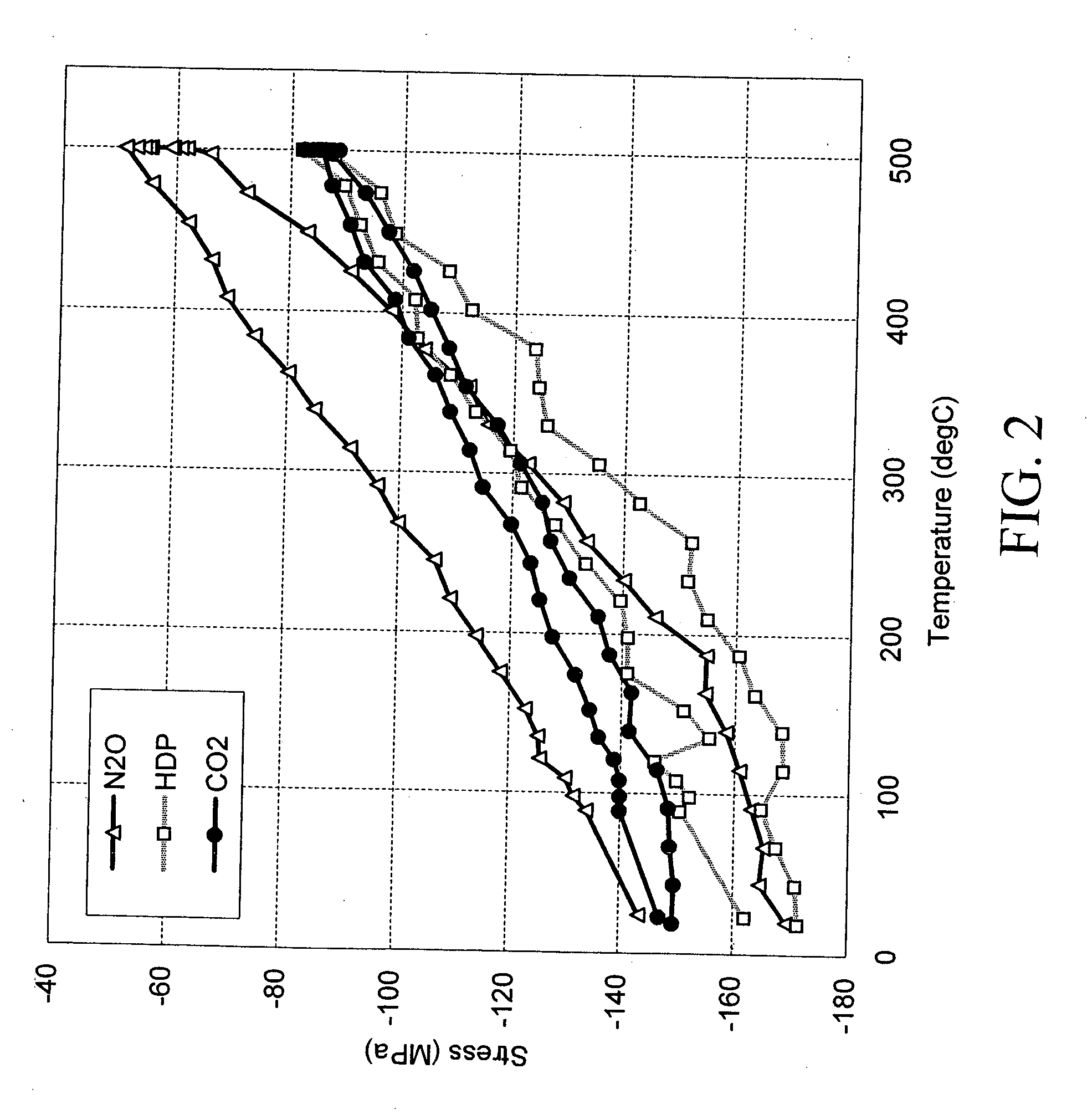
[0052] The capacitive-coupled plasma CVD apparatus shown in FIG. 1 was used for both an embodiment and a comparative example.

[0053] Deposition Conditions for Comparative Example [0054] Silicon source gas: SiH4 (50 sccm) [0055] Silicon and fluorine source gas: SiF4 (90 sccm) [0056] Oxidizing gas: N2O (3000 sccm) [0057] Inert gas: He (800 sccm) [0058] Total pressure: (333 Pa) [0059] Substrate temperature: (390° C.) [0060] The first RF power source (HRF): 13.56 MHz (2.55 W / cm2, 800 W) [0061] The second RF power source (LRF): 430 kHz (1.60 W / cm2, 500 W) [0062] Substrate: Ø200 mm silicon substrate

[0063] Deposition Conditions for Examples [0064] Silicon source gas: SiH4 (40 to 60 sccm) [0065] Silicon and fluorine source gas: SiF4 (80 to 200 sccm) [0066] Oxidizing gas: CO2 (1500 to 5000 sccm) [(SiH4+SiF4) / CO2=0.024 to 0.173][0067] Inert gas: He (800 sccm) [0068] Total pressure: (250 to 350 Pa) [0069] Substrate temperature: (390° C.) [0070] The first RF power source (HRF): 13.56 MHz (0.96...


PUM

PropertyMeasurementUnit
total pressureaaaaaaaaaa
frequencyaaaaaaaaaa
frequencyaaaaaaaaaa

Abstract

A method of forming low-dielectric-constant silicon oxide films by capacitive-coupled plasma CVD comprises: introducing a processing gas comprising SiH4 as a silicon source gas, SiF4 as a fluorine source gas, and CO2 as an oxidizing gas to a reaction chamber at a ratio of (SiH4+SiF4) / CO2 in the range of 0.02 to 0.2 and at a total pressure of 250 Pa to 350 Pa; applying first RF power at a frequency of 10 MHz to 30 MHz and second RF power at a frequency of 400 kHz to 500 kHz by overlaying the two RF powers to generate a plasma reaction field within the reaction chamber; and controlling a flow of the respective gases and the respective RF power outputs.

Description

BACKGROUND OF THE INVENTION [0001] 1. Field of the Invention [0002] The present invention generally relates to semiconductor formation technologies using capacitive-coupled plasma CVD, and particularly relates to a method of forming fluorine-doped low-dielectric-constant silicon oxide films having a low dielectric constant and high thermal stability. [0003] 2. Description of the Related Art [0004] In semiconductor integrated circuits, miniaturization has made progress aiming at increasing speeds and providing more sophisticated features. In multilevel interconnect technologies, aluminum had been conventionally used. As the miniaturization had advanced and interconnects had become minute and long, however, problems have emerged including electromigration during use, i.e., disconnection accidents caused by increased current density relative to minute and long interconnects, or signal delays caused by the resistivity of aluminum or a dielectric constant of an insulating film. [0005] Be...

Claims


Application Information

Patent Timeline
Patent Type & Authority Applications(United States)
IPC IPC(8): H01L21/31
CPCC23C16/401H01L21/02131H01L21/31629H01L21/02274H01L21/02211
Inventor TSUJI, NAOTOIKEDO, YOZONAKANO, RYUHEBIGUCHI, SHUZO
Owner ASM JAPAN
Why Eureka
Try Eureka