LSI package with interface module, transmission line package, and ribbon optical transmission line

a technology of interface module and transmission line, which is applied in the direction of high frequency circuit adaptation, sustainable manufacturing/processing, instruments, etc., can solve the problems of limiting the number of terminals, bottlenecking the performance of personal computers, and moderate improvement of the throughput of the interface between lsis

Inactive Publication Date: 2006-03-09
KK TOSHIBA
View PDF21 Cites 59 Cited by
  • Summary
  • Abstract
  • Description
  • Claims
  • Application Information

AI Technical Summary

Problems solved by technology

However, the pace of improvement in the throughput of an interface between LSIs is moderate, compared with increase in clock frequency, which constitutes a bottleneck in the performance of the personal computer.
However, there is a limit to the increase in the number of terminals because the increase in the number of terminals results in the enlargement of the areas of an LSI and a package to lengthen the internal wiring length, which hinders a high-frequency operation, and therefore the increase in the frequency per terminal becomes a large problem.
On the other hand, the increase in the frequency per terminal results in larger attenuation of an electrical signal and a larger influence of reflection due to impedance mismatch, which imposes a limit on the line length.
The accurate formation of the transmission line on a mounting board causes not only cost increase but also increases in dielectric loss and conductor loss due to a skin effect with an increase in speed, which makes transmission over a sufficient distance difficult.
In the case of Japanese Patent Laid-open Application No. 2004-31455, the optical element is directly bare-chip mounted on an interposer board and optically coupled to an optical waveguide when the interposer board is mounted on the mounting board, so that it is difficult to maintain optical accuracy because of the difference in thermal expansion coefficient between the mounting board and the interposer.
Further, since it is difficult to ensure reliability of the bare optical element, it is necessary to adopt a method of embedding an optical element portion with a transparent resin or the like, for example, at a wavelength used for signal transmission, but there is a problem that this method needs a work on the mounting board, has many restrictions in terms of manufacturing, and costs a lot.
There is another problem that an extra work of attaching the optical waveguide to the mounting board is necessary, which complicates the mounting process, resulting in cost increase.
There is still another problem that when the optical element breaks down, an expensive signal processing LSI has to be also renewed together with the optical element.
Therefore, it is necessary that the LSI package is reflow mounted on the mounting board while the optical component is mounted thereon or the optical component is mounted after the LSI package is reflow mounted on the mounting board, whereby in this structure, the optical component and an assembling material (such as an adhesive) which are easily affected by heat and the reflow mounting at the time of board mounting interfere with each other.
Moreover, mutual interference among soldering of the LSI, soldering of the optical interface module, and, in some cases, soldering of the interposer occurs, which poses a problem in terms of mounting such as the occurrence of restrictions on the mounting procedure.
Because of this reason and so on, the use of the connector for the optical connection tends to enlarge the mechanism.
Namely, an accuracy as high as several micro-meters to 10 micro-meters is required as the mounting accuracy of the optical connector, and hence the holding mechanism of the connector is difficult to downsize, and tends to be upsized.
Therefore, there are a problem of cost increase caused by the complication of the structure, for example, by the formation of a recessed space in a heat sink attached on an upper portion of the LSI, and a problem that it becomes difficult to attach a heat sink for heat release of the optical interface module.
In general, power consumption per terminal tends to become larger with an increase in the frequency of a signal.
Also in this case, there is a problem that since the interface module is soldered, the expensive signal processing LSI has to be also renewed together when the interface module breaks down.
However, such an LSI package as shown in the conventional example has a problem that it is difficult to control the line length of the transmission line to be aerially wired when the LSI package is mounted on the mounting board.
Namely, the length of the transmission line is determined according to the layout design of LSI packages, and in consideration of allowances for attachment to connectors and the LSI packages, the transmission line is cut to a predetermined length and attached, but at this time, it is difficult to reduce a fabrication error to zero, and it is common that a small length error occurs.
Moreover, depending on the difference in thermal expansion coefficient between the mounting board and transmission line, a relative error between the LSI packages, that is, between the wiring length viewed from the board and the transmission line length occurs according to ambient temperature change.
Hence, the transmission line in such a package needs to be formed longer than the predetermined length, but a deflection of the transmission line caused by its extra length is not properly processed.
In such a transmission line package, the above-described fabrication error of the transmission line is absolutely inevitable.
When the transmission line is shorter than the wiring length, the LSI package is pulled by the transmission line, which causes troubles such as poor mounting of the LSI package, breakage of the optical interface or the transmission line, and so on.
When the deflection caused by this extra length becomes several tens of millimeters, in some cases, the aerially wired transmission line is caught by another component of the mounting board or sympathetically vibrates by cooling air from a cooling fan to thereby be damaged at its base portion.
Accordingly, since the deflection of the transmission line caused by the extra length is not properly processed, stress caused by the deflection of the transmission line is applied to the optical interface and the LSI package.
As a result, a problem such that in order to cope with the stress, a pressing mechanism is upsized, tends to occur.

Method used


Image

  • LSI package with interface module, transmission line package, and ribbon optical transmission line
  • LSI package with interface module, transmission line package, and ribbon optical transmission line
  • LSI package with interface module, transmission line package, and ribbon optical transmission line

Examples


first embodiment

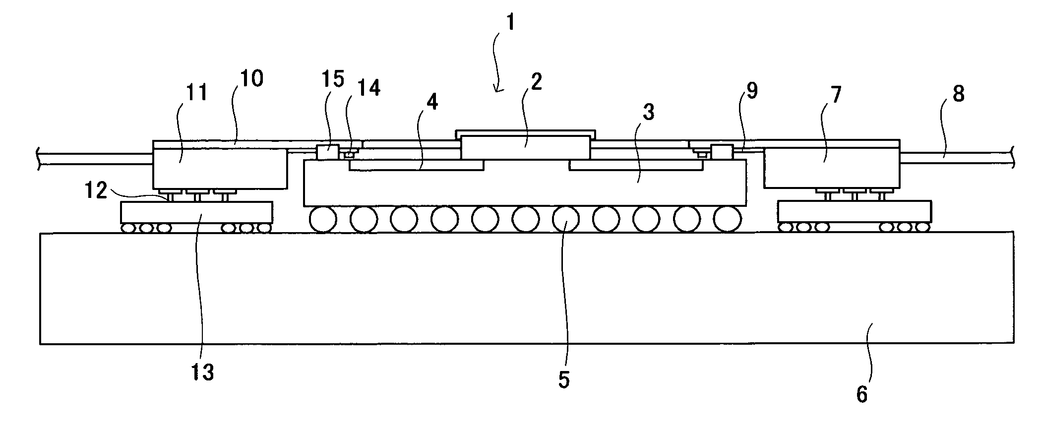
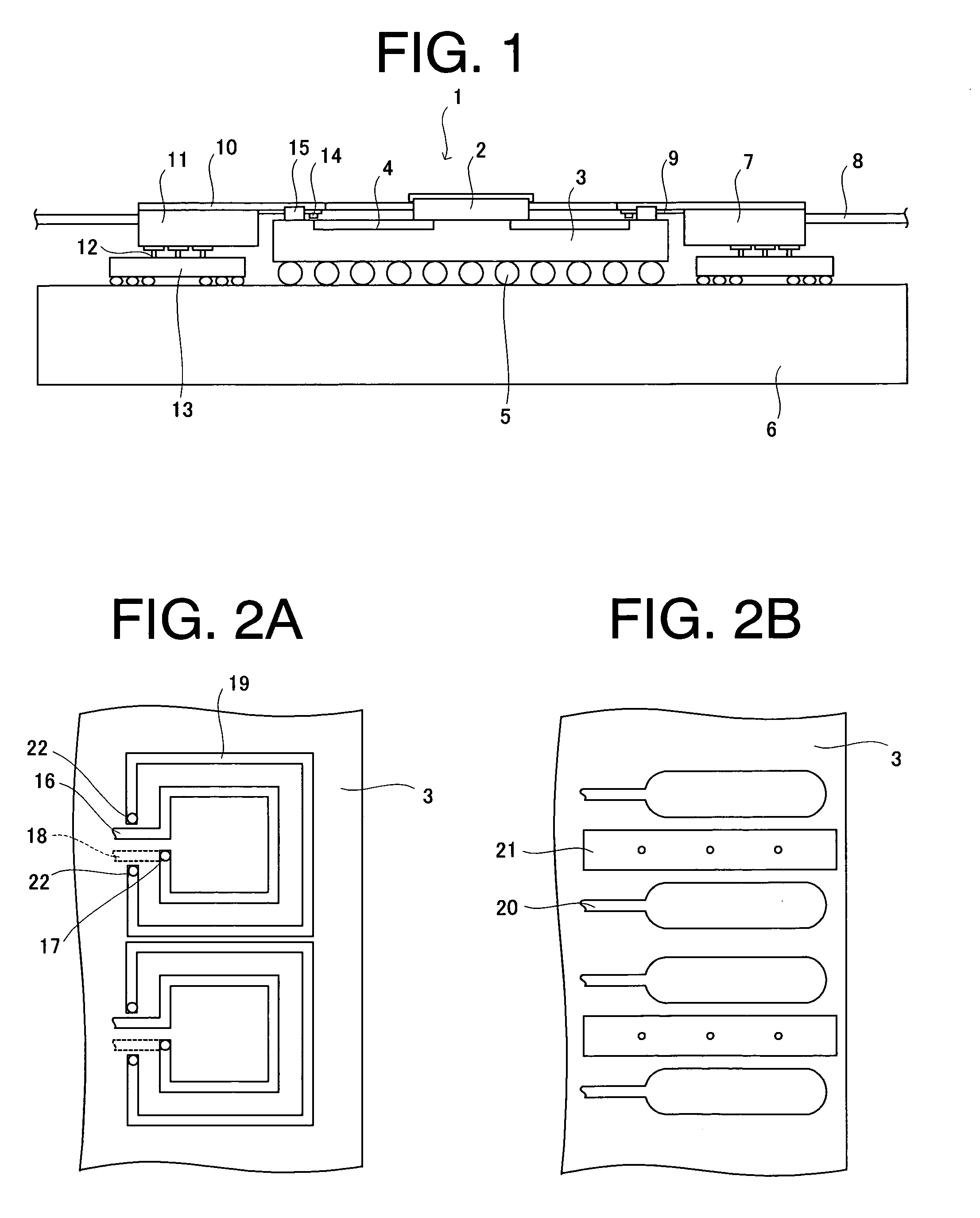
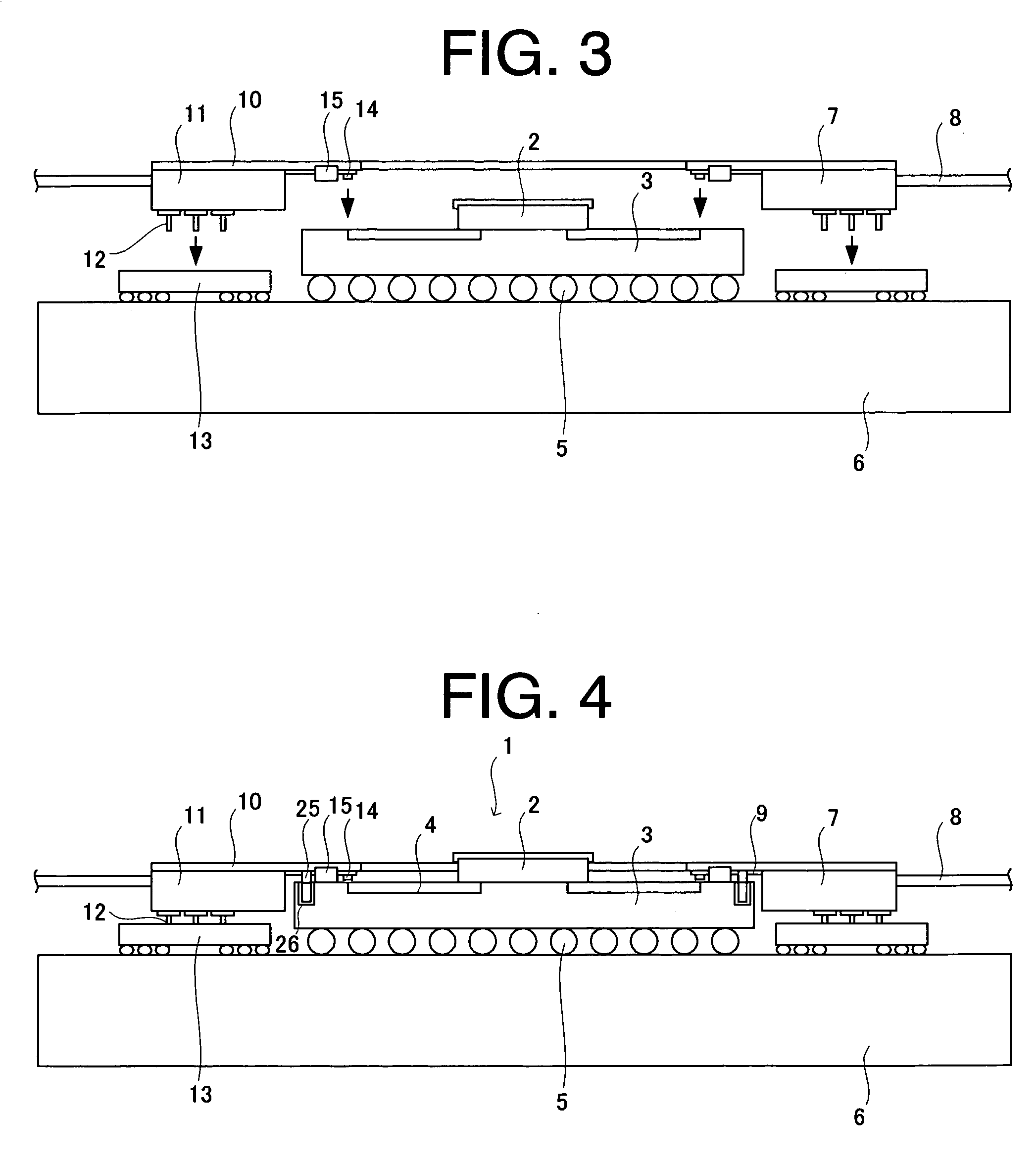
[0060]FIG. 1 is a view showing a schematic structure of an LSI package with an interface module according to a first embodiment of the present invention, FIG. 2A and FIG. 2B are enlarged views of a connection portion of a high-speed signal wire according to the first embodiment of the present invention, FIG. 3 is a view showing a mounting process of the LSI package with the interface module according to the first embodiment of the present invention, and FIG. 4 is a view showing a schematic structure of another LSI package with an interface module according to the first embodiment of the present invention.

[0061] In FIG. 1, numeral 1 denotes an LSI package with an interface module, and the LSI package with the interface module 1 includes a signal processing LSI 2. The signal processing LSI 2 is mounted on an interposer 3, and the signal processing LSI 2 and the interposer 3 are electrically connected.

[0062] A high-speed signal wire 4 is wired in the interposer 3, and the high-speed ...

second embodiment

[0072]FIG. 5 is a view showing a schematic structure of an LSI package with an interface module according to a second embodiment of the present invention, FIG. 6 is a view showing a connecting process of an optical interface module according to the second embodiment of the present invention, and FIG. 7 shows a top view of an interposer with an FPC according to the second embodiment of the present invention. Incidentally, the same portions as shown in FIG. 1 are denoted by the same numerals and symbols, so that the detailed description thereof will be omitted.

[0073] As shown in FIG. 5, an FPC connector 31 (an electrical connector) is mounted on the interposer 3, and an FPC connector 32 (an electrical connector) is mounted on the optical interface module 7. Both ends of the FPC 9 are connected to the FPC connectors 31 and 32, respectively, and electrically connected to an electrical connection terminal (not shown) of the interposer 3 and an electrical connection terminal (not shown) ...

third embodiment

[0078]FIG. 8 is a view showing a schematic structure of an LSI package with an interface module according to a third embodiment of the present invention, FIG. 9 is an enlarged view of a connection portion of a high-speed signal wire according to the third embodiment of the present invention, and FIG. 10 is a view showing a connecting process of an optical interface module according to the third embodiment of the present invention. Incidentally, the same portions as shown in FIG. 1 are denoted by the same numerals and symbols, so that the detailed description thereof will be omitted.

[0079] As shown in FIG. 8, in this embodiment, the interposer 3 is connected to a socket 42, which is connected to the mounting board 6 by solder bumps 41, by input / output pins 43 (a socket connection terminal pin). More specifically, jacks 44 fittable with the input / output pins 43 are formed in the socket 42, and by fitting the input / output pins 43 into the jacks 42, the interposer 3 is connected to the...


PUM


Abstract

According to an aspect of the present invention, there is provided an LSI package with an interface module including: an interposer, on which a signal processing LSI is mounted, having a mounting board connecting electrical terminal; and an interface module having a transmission line to wire a high-speed signal to the exterior and a socket connecting electrical terminal corresponding to a mounting board connecting socket, in which the interposer and the interface module have at least either loop electrodes or plate electrodes, respectively, and the interposer and the interface module are electrically connected by inductive coupling, electrostatic coupling, or combined coupling of these two couplings by at least either the loop electrodes or the plate electrodes.

Description

CROSS-REFERENCE TO RELATED APPLICATIONS [0001] This application is based upon and claims the benefit of priority from the prior Japanese Patent Applications No. 2004-237722 and 2004-237723, filed on Aug. 17, 2004, respectively; the entire contents of which are incorporated herein by reference. BACKGROUND OF THE INVENTION [0002] 1. Field of the Invention [0003] The present invention relates to an LSI package with an interface module including an interface module to wire a high-speed signal to an exterior, a transmission line package applied to high-speed LSI mounting, and a ribbon optical transmission line. [0004] 2. Description of the Related Art [0005] In recent years, the clock frequency of an LSI has been getting increasingly higher and a CPU for a personal computer that is operated with a frequency of GHz or higher has been put into practical use. However, the pace of improvement in the throughput of an interface between LSIs is moderate, compared with increase in clock frequenc...

Claims


Application Information

Patent Timeline
Patent Type & Authority Applications(United States)
IPC IPC(8): H05K7/10
CPCG02B6/2552G02B6/4201G02B6/43H05K1/0239H05K1/181H05K3/301H01L2924/0002H05K2201/10325H05K2201/10522H05K2201/10734H01L2924/00G02B6/4269G02B6/428Y02P70/50H01L25/00H05K1/02
Inventor HAMASAKI, HIROSHIFURUYAMA, HIDETONUMATA, HIDEOTAKUBO, CHIAKI
Owner KK TOSHIBA
Why Eureka
Try Eureka