Method for generating identification code of semiconductor device, method for identifying semiconductor device and semiconductor device

a technology for identification codes and semiconductor devices, applied in the direction of digital data processing details, measurement devices, instruments, etc., can solve the problems of consuming time and cost, affecting the identification of semiconductor devices, and complicated operation of writing information

Inactive Publication Date: 2006-03-09
PANASONIC CORP
View PDF7 Cites 24 Cited by
  • Summary
  • Abstract
  • Description
  • Claims
  • Application Information

AI Technical Summary

Benefits of technology

[0007] It is therefore an object of the present invention to provide a low-cost method for identifying a semiconductor device performed by using the semiconductor device itself, and a method for generating an identification code for use in that method.
[0009] First logical values output after power has been supplied to a semiconductor device are greatly affected by variations in fabrication of the semiconductor device as compared to logical values output during normal operation. Accordingly, logical values unique to the respective elements constituting the semiconductor device are obtained, so that an identification code enabling more accurate identification of the semiconductor device is obtained. The identification code is obtained by using the semiconductor device itself, so that simplification and cost reduction of the identification are achieved. The obtained initial pattern code is based on variations in transistor characteristics inherently provided in the semiconductor device. Accordingly, identification information is easily obtained in any one of a wafer state, a package state after assembly and a chip state.
[0011] In the step (b), a mask code in which only the logical value output from said each unstable element is “0” may be generated as a portion of the identification code. In this case, more accurate identification is performed by using the unique code and the mask code. Specifically, AND operation of a unique code (target unique code) of a semiconductor device to be identified and a mask code for comparison (comparative mask code) is performed and AND operation of a mask code (target mask code) of the semiconductor device to be identified and a unique code for comparison (comparative unique code) is performed. The results of these operations are compared with each other, so that the semiconductor device is identified more accurately.
[0012] Before the step (a), “0” or “1” may be written in all the elements before the power is shut off and before the step (c), “0” or “1” may be written in all the elements before the power is shut off. In this case, in the step (a), unstable elements are affected by charge remaining at initialization to output “0” when “0” is written and output “1” when “1” is written. This further ensures detection of unstable elements.
[0023] First logical values output after power has been supplied to a semiconductor device are greatly affected by variations in fabrication of the semiconductor device as compared to logical values output during normal operation. Accordingly, in the identification information generating circuit, logical values unique to the respective elements constituting the circuit are obtained. As a result, the semiconductor device enables more accurate identification.

Problems solved by technology

In the method with which identification information on individual semiconductor devices is stored by using a laser trimmer, however, laser trimmer apparatus needs to be introduced and operation of writing information is complicated.
Therefore, either method consumes time and cost.
However, this method is limited to identification of a semiconductor device that includes TFTs formed on a substrate having an insulating surface.
Therefore, the method has a drawback of incapability of being used as a method for identifying a general semiconductor device constituted by MOS transistors or bipolar transistors formed on a silicon substrate.

Method used


Image

  • Method for generating identification code of semiconductor device, method for identifying semiconductor device and semiconductor device
  • Method for generating identification code of semiconductor device, method for identifying semiconductor device and semiconductor device
  • Method for generating identification code of semiconductor device, method for identifying semiconductor device and semiconductor device

Examples


embodiment 1

[0038] Methods for identifying semiconductor devices (chips) according to the present invention are based on the following idea. In a semiconductor integrated circuit including a logic circuit or an system LSI, a large number of flip-flops, RAMs or static random access memories (SRAMs) formed by MOS processes or CMOS processes are generally provided. Each of these circuits is constituted by a plurality of MOS transistors and fabrication conditions thereof vary depending on the time, so that the transistor pattern size and the impurity diffusion concentration vary one wafer to another in a lot or depending on the position in a wafer. These variations in fabrication processes cause variations in operation output characteristics such as a variation in a threshold voltage even among transistors designed to be identical in specifications.

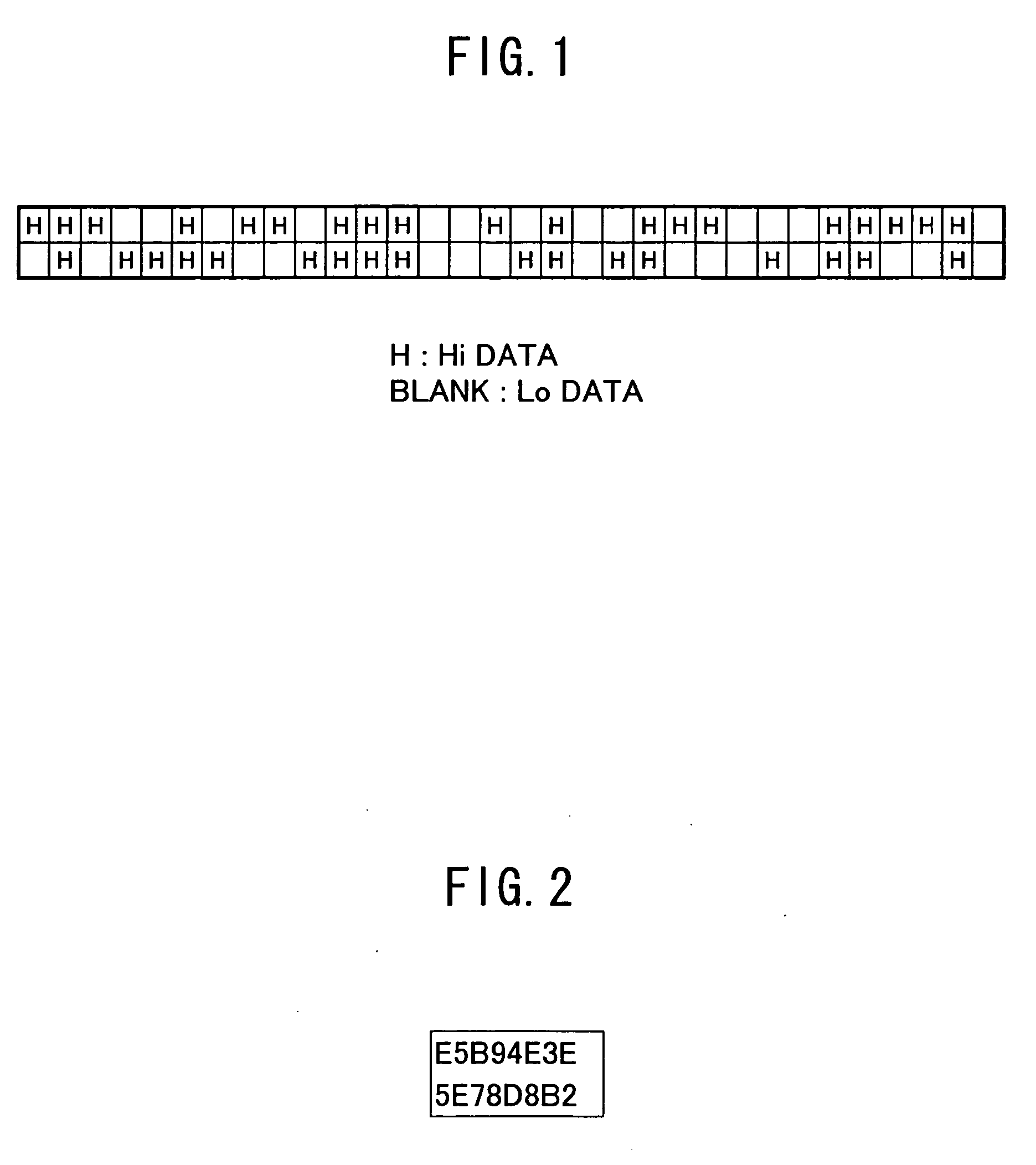
[0039] According to the present invention, in a semiconductor device including circuits each outputting a binary value of high (Hi) / low (Lo) (or 1 / 0), ...

embodiment 2

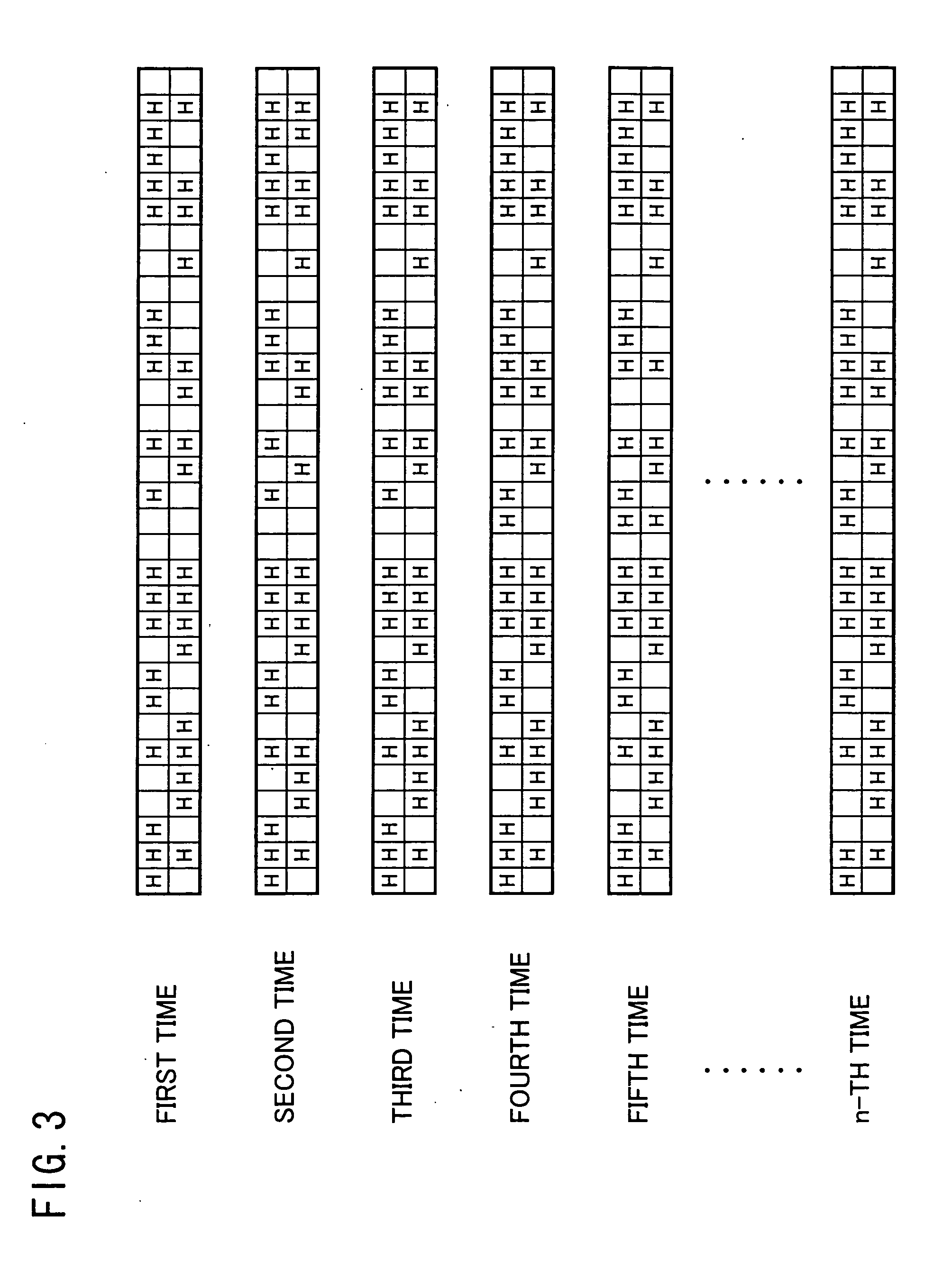
[0045] As described in the first embodiment, with a method for generating a chip identification code according to the present invention, an initial pattern code is obtained from signals output from SRAMs at specified addresses at power-on of a device and the obtained initial pattern code is used as an identification code. However, the same signal (data) is not always output from a specified address at the power-on. In particular, with respect to unstable memory cells exhibiting variations in characteristics such as transistor characteristics and memory cell electrical characteristics, outputs from these memory cells can vary, so that the output of Hi / Lo varies at every power-on in some cases. To prevent this variation, a method for ensuring identification of even a chip including such unstable memory cells is provided in this embodiment.

[0046]FIG. 3 shows tables illustrating n initial pattern codes repeatedly obtained by the method of the first embodiment using SRAMs including unst...

embodiment 3

[0063] In this embodiment, a method for ensuring generation of a stable ID code even when outputs from memory cells such as flip-flops or SRAMs vary through various processes such as packaging after the first ID code has been obtained.

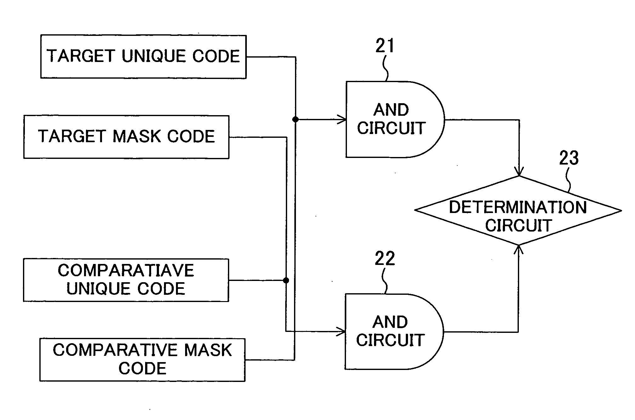
[0064] In this embodiment, operation in which all the memory cells in a semiconductor device whose ID code is to be obtained are initialized to be “1” or “0” and then power is turned off and on again is repeatedly performed, so that an initial pattern code as shown in FIG. 3 is obtained a plurality of times. With this method, unstable memory cells are affected by charge remaining at initialization, although output “1” when all the memory cells are initialized to be “1” and output “0” when all the memory cells are initialized to be “0”. When operation is performed on the initial pattern codes obtained by using the circuit shown in FIG. 6, a unique code from which the unstable bits have been eliminated as Lo is generated. This method further ensures det...


PUM


Abstract

A semiconductor device including memory cells such as flip-flops, RAMs or SRAMs is powered on, and first logic signals of Hi or Lo output from the respective memory cells are obtained. A combination of the logic signals is used as a unique identification code for identifying a semiconductor device.

Description

CROSS-REFERENCE TO RELATED APPLICATION [0001] The disclosure of Japanese Patent Application No. 2004-241987 filed on Aug. 23, 2004 including specification, drawings and claims is incorporated herein by reference in its entirety. BACKGROUND OF THE INVENTION [0002] The present invention relates to a method for generating an identification code of a semiconductor device in which a large number of circuits outputting binary values of Hi / Lo, e.g., flip-flops or random access memories (RAMs), are formed on a substrate, a method for identifying a semiconductor device, and a semiconductor device. [0003] In management of a fabrication process of a semiconductor integrated circuit and failure analysis of the circuit, it is necessary to identify individual dies (chips) formed out of a semiconductor substrate. For example, to analyze a cause of a failure of an integrated circuit after shipment and take measures against the failure, examination going back to history of a semiconductor fabricatio...

Claims


Application Information

Patent Timeline
Patent Type & Authority Applications(United States)
IPC IPC(8): G06F3/00
CPCG01R31/31722G11C7/20G06F7/588G11C2029/4402H01L21/67294G11C16/20H01L21/02
Inventor YAMAGUCHI, YOSHIAKIFURUKAWA, TATSUYASHIMOKAWA, KOICHI
Owner PANASONIC CORP
Why Eureka
Try Eureka