Copper-metallized integrated circuits having electroless thick copper bond pads

a technology of copper-metallized integrated circuits and contact pads, which is applied in the direction of layered products, transportation and packaging, chemical instruments and processes, etc., can solve the problems of bare copper bond pads being susceptible to corrosion, copper oxide films overlying metallic copper cannot be easily broken by a combination, and severe inhibiting the reliable attachment of bonding wires

Active Publication Date: 2007-02-08
TEXAS INSTR INC
View PDF1 Cites 10 Cited by
  • Summary
  • Abstract
  • Description
  • Claims
  • Application Information

AI Technical Summary

Benefits of technology

[0009] Embodiments of the present invention are related to wire-bonded IC assemblies, semiconductor device packages, surface mount and chip-scale packages. Other embodiments are related to interconnecting wiring boards. It is a technical advantage that the invention offers a low-cost method of sealing the bond pad against moisture and delamination, and thus for protecting the integrated circuit against corrosion and stress-related contact failure. A further technical advantage includes the uniform copper surface produced by electroless plating, enabling a controlled uniform nickel layer thickness.

Problems solved by technology

For IC bond pads made of copper, the formation of thin copper(I)oxide films during the manufacturing process flow severely inhibits reliable attachment of bonding wires, especially for conventional gold-wire ball bonding.
In contrast to aluminum oxide films overlying metallic aluminum, copper oxide films overlying metallic copper cannot easily be broken by a combination of thermo-compression and ultrasonic energy applied in the bonding process.
As further difficulty, bare copper bond pads are susceptible to corrosion.
This process, though, has a number of drawbacks such as added cost and the risk of inadvertent scratching or smearing of the aluminum, causing electrical shorts.
Alternative processes based on the concept of depositing layers of nickel, palladium, and gold on the copper, which are reliably bondable, have until now run into technical problems, such as insufficient adhesion among the various metal layers and insulating materials, unexpected corrosion and chemical undercuts, or void formation with long-term risks of opens in fine interconnecting copper lines.
Specifically, plating issues have been encountered when bare copper bond pads are plated electrolessly with layers of nickel and of palladium, followed by a layer of immersion gold.
Notable among these issues are: widely varying nickel layer thickness, when the copper surface condition is variable; voids in the copper bond pad caused by the process of palladium surface activation for the copper; and undercut, or crevice, corrosion of the copper under the protective overcoat during the palladium activation and plating.

Method used


Image

  • Copper-metallized integrated circuits having electroless thick copper bond pads
  • Copper-metallized integrated circuits having electroless thick copper bond pads
  • Copper-metallized integrated circuits having electroless thick copper bond pads

Examples


Embodiment Construction

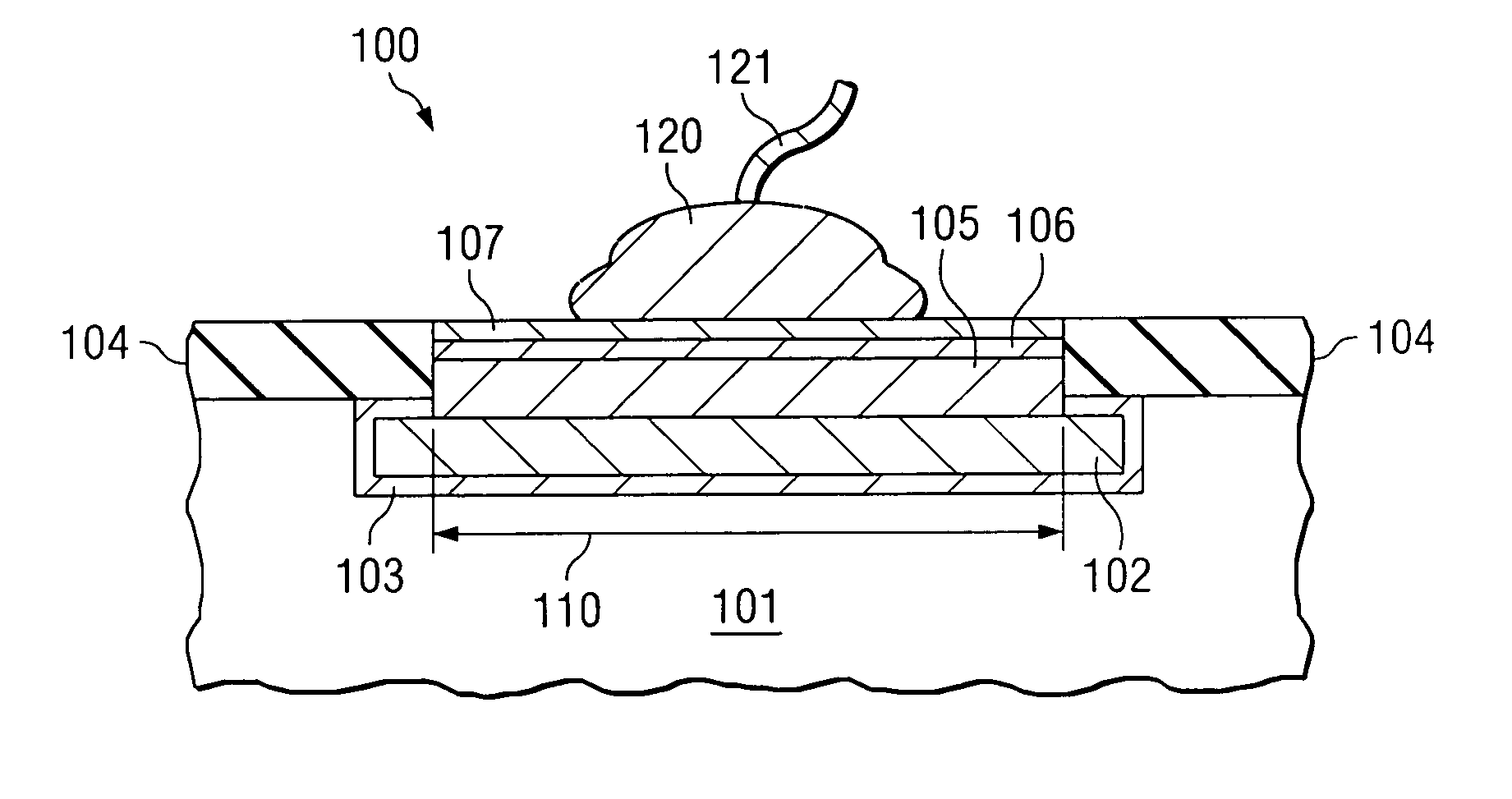
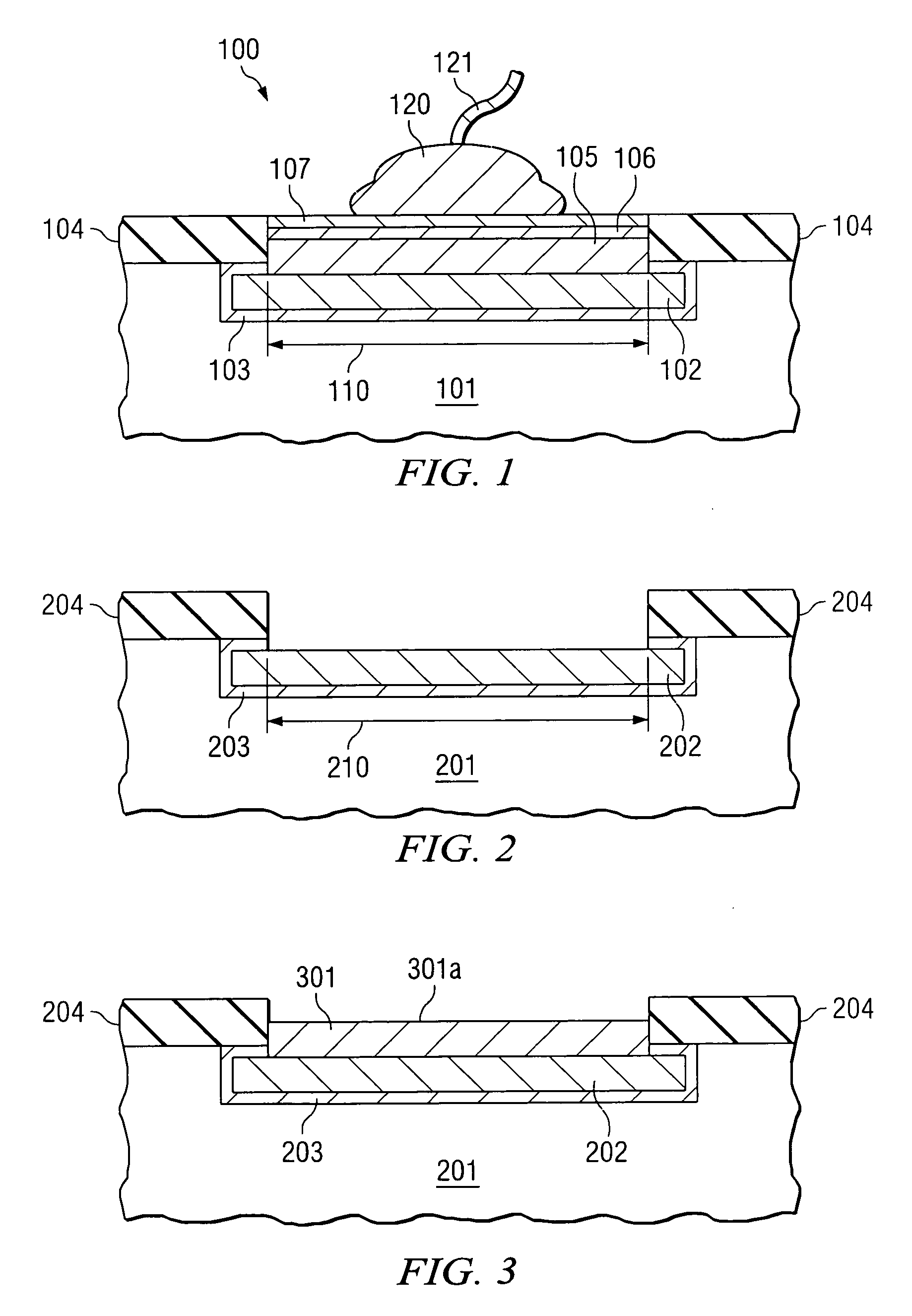
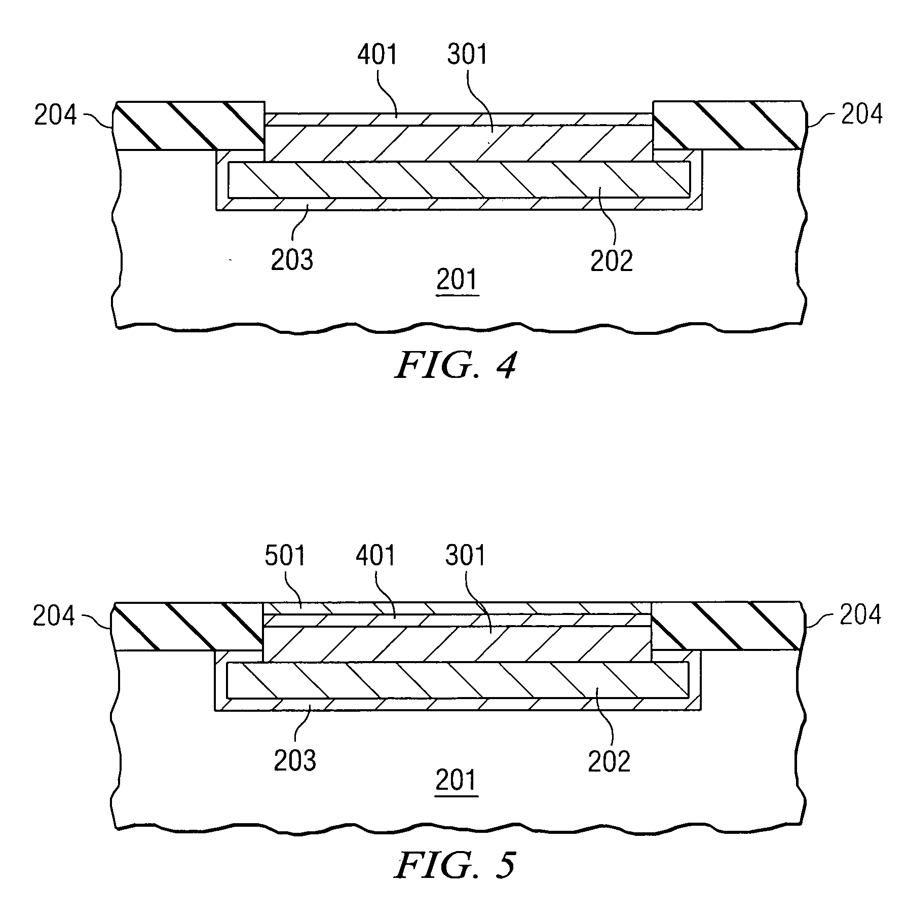
[0017] The schematic cross section of FIG. 1 illustrates a bond pad generally designated 100 of a semiconductor device, completed according to the process flow of the invention and with a wire bond attached. A semiconductor chip 101 has interconnecting traces 102 made of a first copper layer. For an integrated circuit, first copper layer 102 has preferably a thickness (first thickness) in the range from about 0.2 to 1.0 μm. In order to prevent outdiffusion of the copper, trace 102 is preferably surrounded by a barrier metal layer 103. Barrier metal layer 103 is typically tantalum nitride in the thickness range from about 20 to 50 nm. Semiconductor chip 101 is protected by an insulating overcoat 104, typically made of silicon nitride, silicon oxynitride, silicon carbide, polyimide, or stacks of these or related insulators; a preferred thickness range is from about 0.5 to 1.0 μm.

[0018] As FIG. 1 shows, trace 102 of the first copper layer is selectively exposed by the window 110 in th...


PUM

PropertyMeasurementUnit
thicknessaaaaaaaaaa
thicknessaaaaaaaaaa
thicknessaaaaaaaaaa

Abstract

A metal structure (100) for a contact pad of a semiconductor device, which has interconnecting traces of a first copper layer (102). The substrate is protected by an insulating overcoat (104). In the structure, the first copper layer of first thickness and first crystallite size is selectively exposed by a window (110) in the insulating overcoat. A layer of second copper (105) of second thickness covers conformally the exposed first copper layer. The second layer is deposited by an electroless process and consists of a transition zone, adjoining the first layer and having copper crystallites of a second size, and a main zone having crystallites of the first size. The second thickness is selected so that the distance a void from the second layer can migrate during the life expectancy of the structure is smaller than the combined thicknesses of the first and second layers. A layer of nickel (106) is on the second copper layer, and a layer of noble metal (107) is on the nickel layer.

Description

FIELD OF THE INVENTION [0001] The present invention is related in general to the field of metallurgical systems with application to electronic systems and semiconductor devices and more specifically to structure and methods for integrated circuit contact pads of copper-metallized integrated circuits. DESCRIPTION OF THE RELATED ART [0002] It is a continuing trend in the semiconductor industry to miniaturize integrated circuits (ICs). As a consequence of this trend, the RC time constant of the interconnection between active circuit elements increasingly dominates the achievable IC speed-power product. Consequently, there is a strong need to replace the relatively high impedance of the interconnecting aluminum metallization by the lower impedance of metals such as copper. [0003] For IC bond pads made of copper, the formation of thin copper(I)oxide films during the manufacturing process flow severely inhibits reliable attachment of bonding wires, especially for conventional gold-wire ba...

Claims


Application Information

Patent Timeline
Patent Type & Authority Applications(United States)
IPC IPC(8): B32B15/20
CPCB32B15/20H01L24/05H01L24/45H01L24/48H01L2224/04042H01L2224/05083H01L2224/05147H01L2224/05155H01L2224/05164H01L2224/05644H01L2224/05655H01L2224/05664H01L2224/45124H01L2224/45144H01L2224/45147H01L2224/48463H01L2924/01013H01L2924/01014H01L2924/01028H01L2924/01029H01L2924/01031H01L2924/01032H01L2924/01046H01L2924/01047H01L2924/01073H01L2924/01075H01L2924/01078H01L2924/01079H01L2924/04953H01L2924/05042H01L2924/14H01L2924/3011H01L2924/01033H01L2224/48755H01L2224/48764H01L2224/48644H01L2224/48655H01L2224/48664H01L2224/48844H01L2224/48855H01L2224/48864Y10T428/1291Y10T428/12889Y10T428/12944Y10T428/12896Y10T428/12528Y10T428/12875Y10T428/12458Y10T428/12903H01L2924/00014H01L2924/00H01L2224/48744H01L2224/45014H01L2924/206
Inventor TEST, HAWARD R.ABBOTT, DONALD C.
Owner TEXAS INSTR INC
Why Eureka
Try Eureka