Multispectral imaging chip using photonic crystals

Active Publication Date: 2006-03-16
RAYTHEON CO
View PDF4 Cites 203 Cited by
  • Summary
  • Abstract
  • Description
  • Claims
  • Application Information

AI Technical Summary

Benefits of technology

[0012] Combining spectral tunability at the cell or pixel level on an FPA with an integrated signal processing layer reduces the data rate by processing only certain spatial pixels over a spectral extent containing information relevant to desired targets. An on-chip processor controls the AFPA's read out integrated circuit (ROIC) to read out the detected photons at a specified spatial resolution and integration period. The on-chip processor also controls the tuning mechanisms to select specific passbands and resolutions in the different cells independently. For example, the on-chip processor may (a) based on a priori knowledge of the scene and/or possible anomalies, set an initial configuration for the ROIC to read out the detected photons at a specified spatial resolution and integration period and for the tuning mechanism to set the passband to a specified central wavelength and bandwidth in the

Problems solved by technology

However, multispectral imagers suffer from limitations, including high mass, volume, and power requirements, as well as a “fire hose” of data to process off line.
None of these approaches are suitable for the necessary miniaturization needed for pixel-by-pixel tuning.
Also this method results in poor wavelength selectivity and provides, at most, only a few different wavebands.
In the latter approach, drawbacks include detector-to-detector image registration requirements and complex opto-m

Method used


Image

  • Multispectral imaging chip using photonic crystals
  • Multispectral imaging chip using photonic crystals
  • Multispectral imaging chip using photonic crystals

Examples


Embodiment Construction

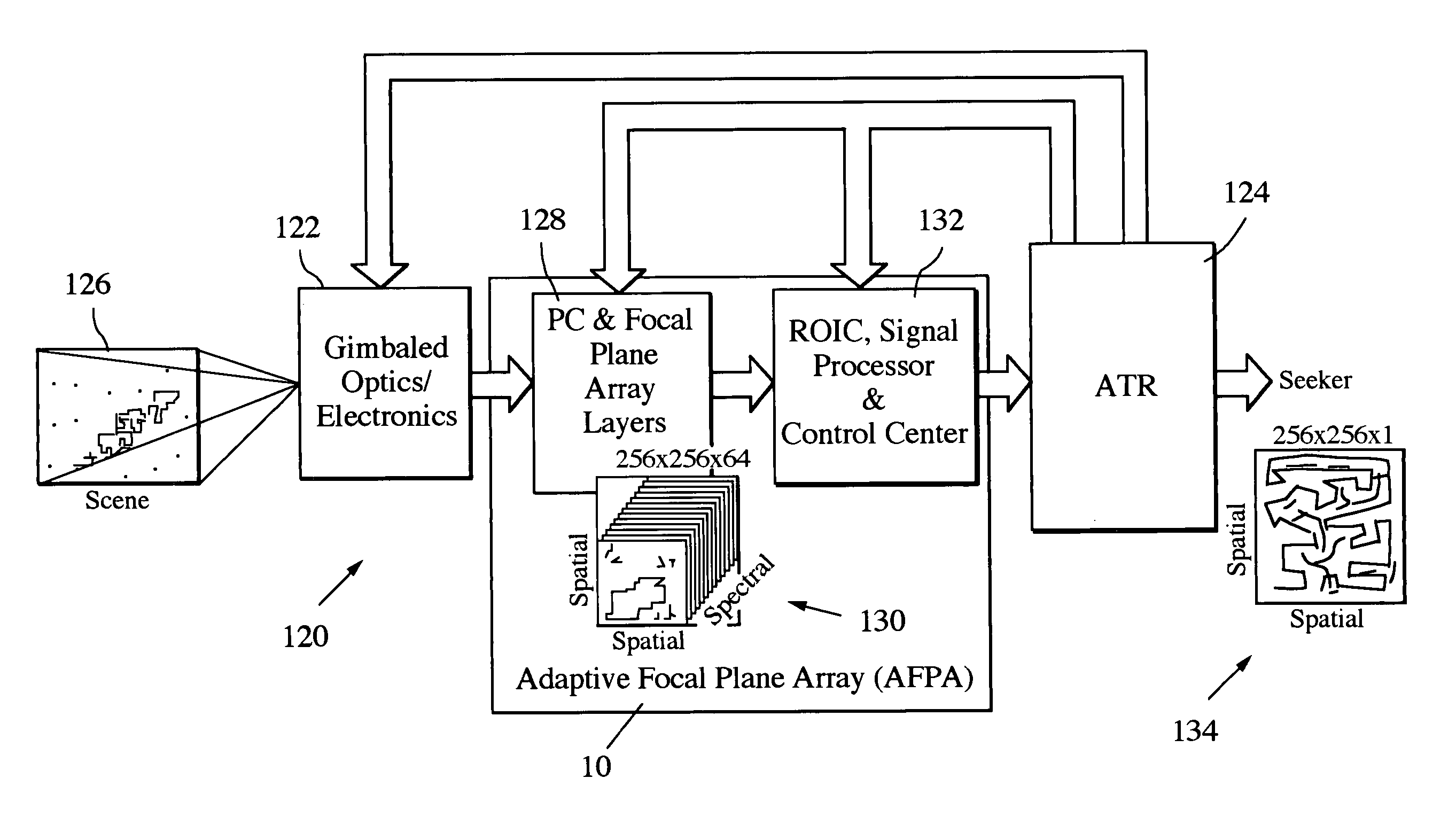
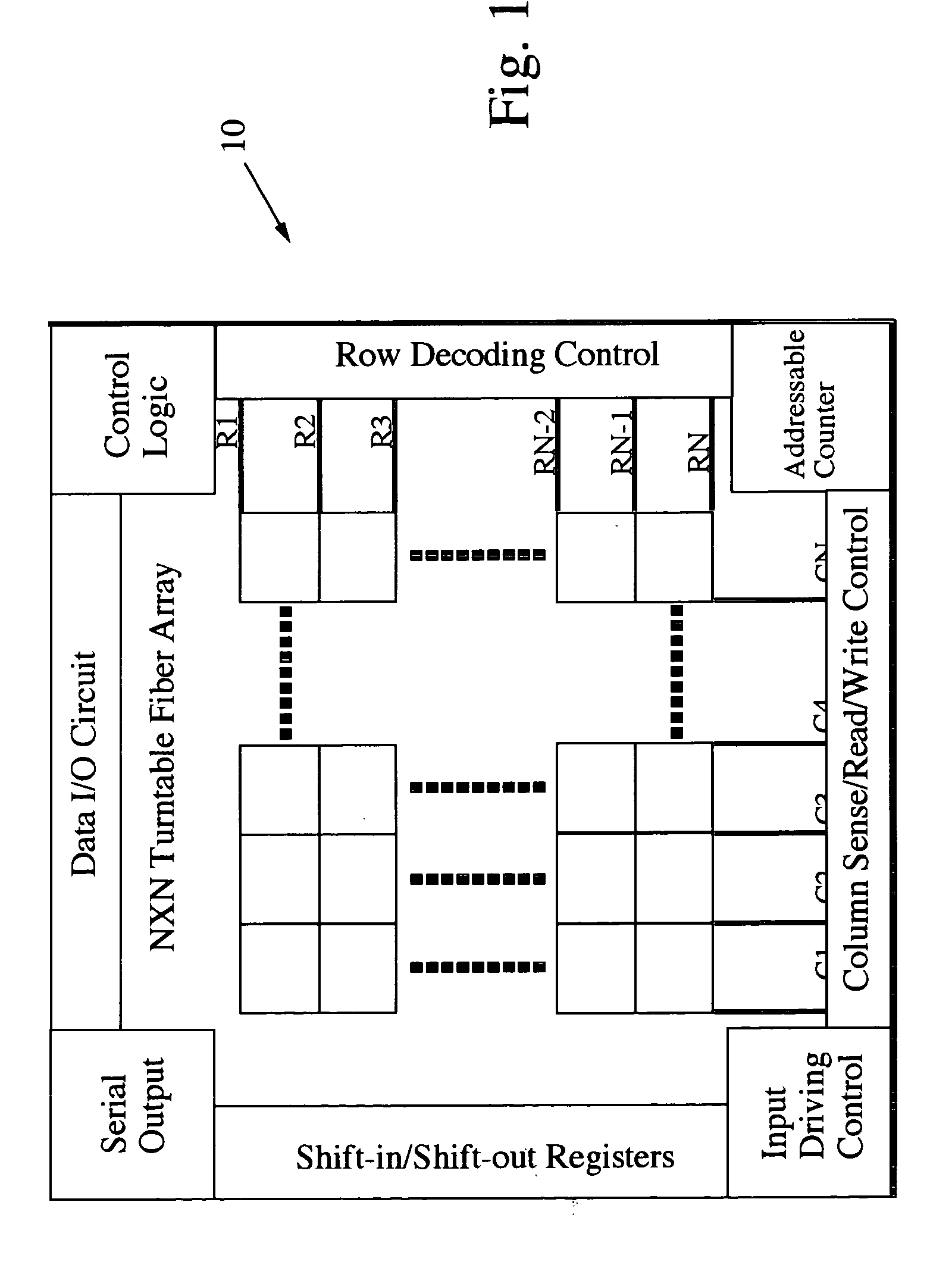
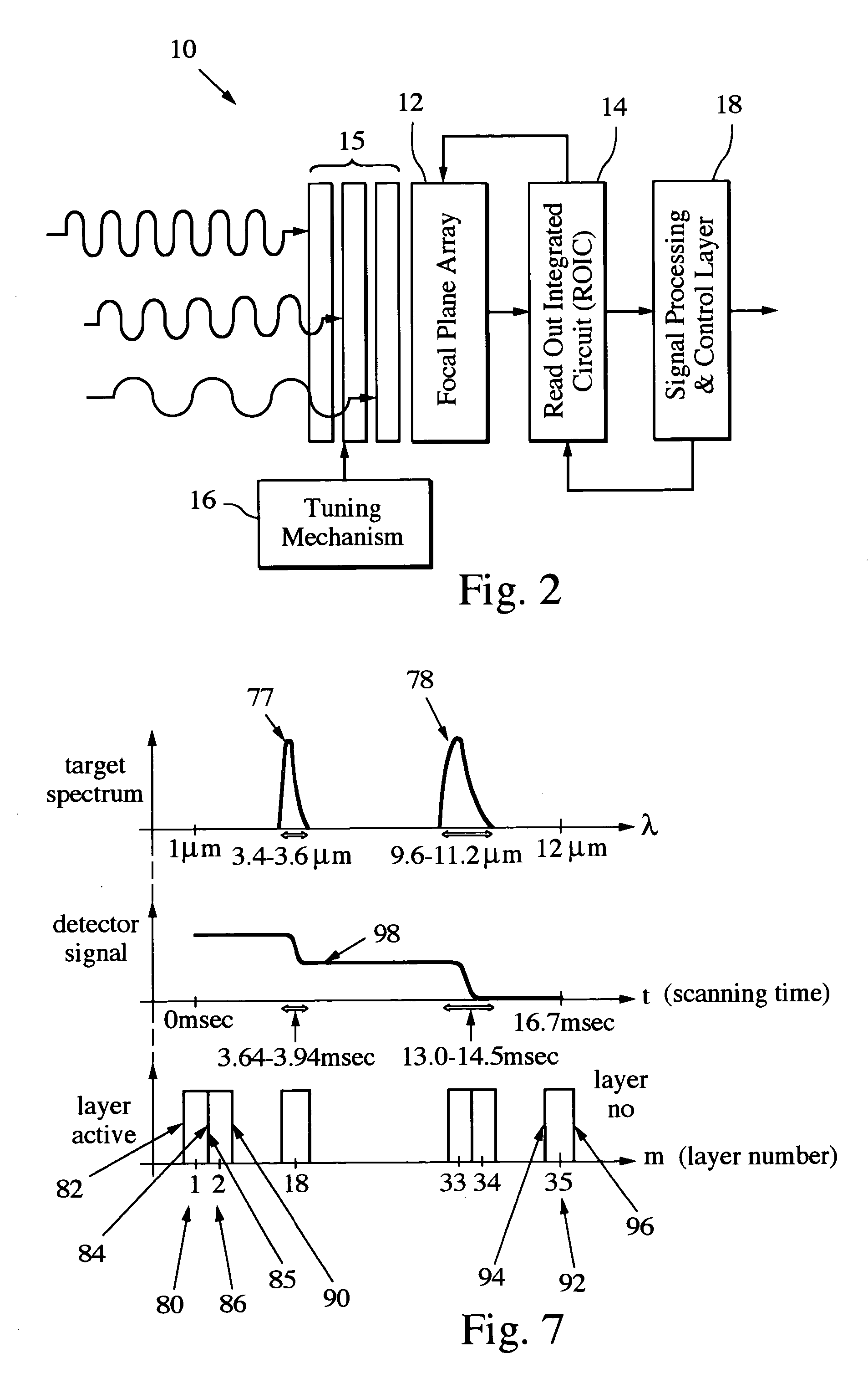
[0023] The present invention describes an approach for “multispectral imaging on a chip” with real-time, pixel-by-pixel spectral selectivity in different electromagnetic wavebands in the form of an Adaptive Focal Plane Array (AFPA). The AFPA exhibits low mass, volume and power requirements, and is capable of intelligently sparsening the tremendous amount of information generated by multispectral sensors. The AFPA marries the technologies of photonic crystals (PCs), broadband detectors and signal processing on-chip. Spectral tuning is accomplished by switching the PC behavior of specific layers on / off and / or by moving the band gaps, either by using an electro-optically active component or by deforming the structure. Each PC layer is responsible for coverage of a portion of the broad operating waveband. Spatial agility is achieved in a processing layer integrated with the Read Out Integrated Circuit (ROIC) layer. Spectral agility enables bandwidth changes as a function of light level....


PUM


Abstract

On-chip multispectral imaging and data management is provided in the form of an Adaptive Focal Plane Array (AFPA) that is capable of spectral tunability at the pixel level. Layers of photonic crystals are registered with pixels of a broadband focal plane array. Spectral tuning is accomplished by switching the photonic crystal layers on/off and/or by changing their material structure to tune their photonic band gaps and provide a passband for incident photons. The photonic crystal layers are preferably segmented to independently address different regions or “cells” of pixels down to a pixel-by-pixel resolution. The AFPA may simultaneously sense different regions of a scene at different spectral wavelengths, spatial resolutions and sensitivities.

Description

CROSS-REFERENCE TO RELATED APPLICATIONS [0001] This application claims benefit of priority under 35 U.S.C. 119(e) to U.S. Provisional Application No. 60 / 471,580 entitled “Pixel-by-Pixel Multispectral Sensing on a Chip: The Adaptive Focal Plane Array” and filed on Feb. 10, 2004, the entire contents of which are incorporated by reference.BACKGROUND OF THE INVENTION [0002] 1. Field of the Invention [0003] This invention relates to on-chip multispectral imaging and more specifically to the incorporation of photonic crystals and integrated processing capability with a focal plane array to provide spectral tunability and spatial agility in the form of an Adaptive Focal Plane Array (AFPA). [0004] 2. Description of the Related Art [0005] Multispectral imagers flown on aircraft and satellite platforms have provided a wealth of information, ranging from military strategic targets to crop assessments. Multispectral image processing has demonstrated high target detection with low false-alarm ra...

Claims


Application Information

Patent Timeline
IPC IPC(8): H01L27/00G02F1/01H01L27/14
CPCB82Y20/00G02B6/1225G02F1/03H04N5/345H01L27/14625H04N5/33H04N5/332G02F2202/32H04N23/11H04N25/44
Inventor GARROOD, DENNIS J.SHAH, NITESH N.BARKER, DELMAR L.SCHMITT, HARRY A.
Owner RAYTHEON CO
Why Eureka
Try Eureka