Method of etching metals with high selectivity to hafnium-based dielectric materials

Inactive Publication Date: 2006-03-23
APPLIED MATERIALS INC
View PDF14 Cites 30 Cited by
  • Summary
  • Abstract
  • Description
  • Claims
  • Application Information

AI Technical Summary

Benefits of technology

[0010] The present invention is a method of plasma etching a metal layer (e.g., titanium (Ti), tantalum (Ta), tungsten (W), and the like) or a metal-containing layer (e.g., tantalum silicon nitride (TaSiN), titanium nitride (TiN), tungsten nitride (WN), and the like) formed on

Problems solved by technology

However, many processes that are used to etch metal layers (e.g., titanium (Ti), tantalum (Ta), titanium nitride (TiN) and tantalum nitride (TaN)) typically have a low etch selectivity for underlying thin layers of hafnium-based high-K dielectric materials (

Method used


Image

  • Method of etching metals with high selectivity to hafnium-based dielectric materials
  • Method of etching metals with high selectivity to hafnium-based dielectric materials
  • Method of etching metals with high selectivity to hafnium-based dielectric materials

Examples


Embodiment Construction

[0017] The present invention is a method of plasma etching a metal layer (e.g., titanium (Ti), tantalum (Ta), and the like) or a metal-containing layer (e.g., tantalum silicon nitride (TaSiN), titanium nitride (TiN), and the like) formed on a hafnium-based dielectric material. The metal / metal-containing layer is etched using a gas mixture comprising a halogen-containing gas and a fluorine-containing gas. The fluorine within the mixture provides a high etch selectivity for the hafnium-based dielectric material.

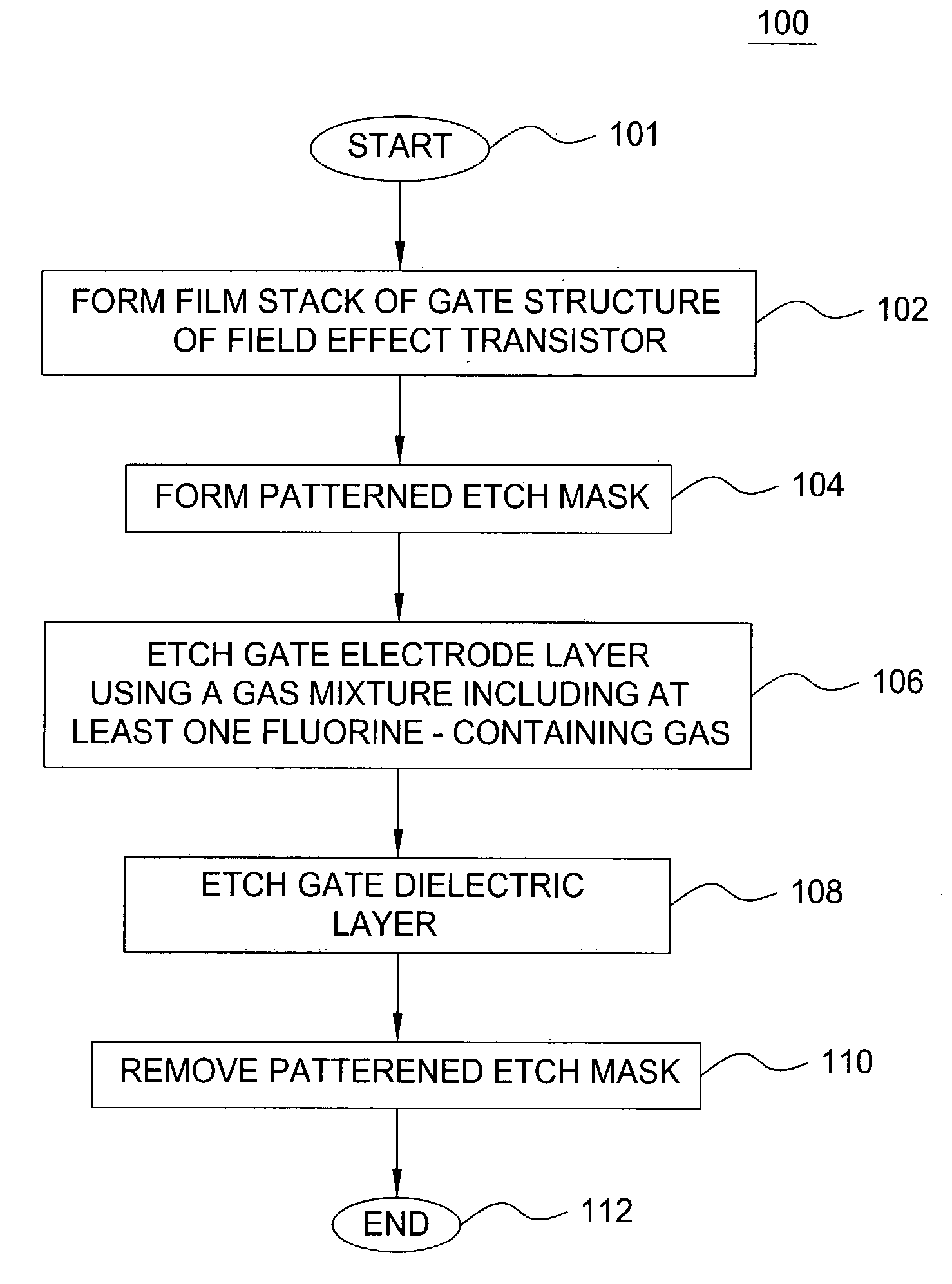
[0018]FIG. 1 depicts a flow diagram of one embodiment of the inventive method for fabricating a gate structure of a CMOS transistor as sequence 100. The sequence 100 includes the processes that are performed upon a film stack of the gate structure during fabrication of the CMOS transistor.

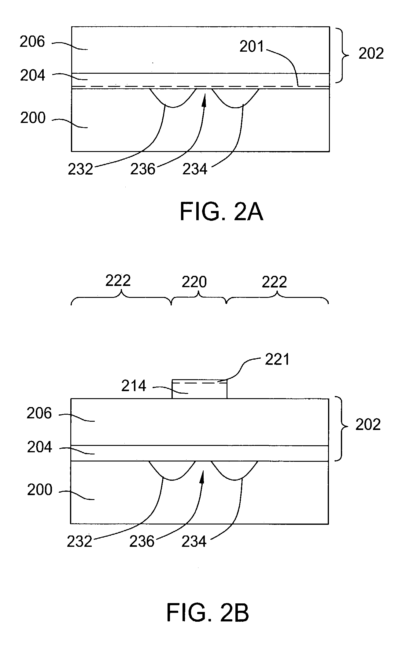
[0019]FIGS. 2A-2F depict a series of schematic, cross-sectional views of a substrate having a film stack of the gate structure being fabricated using sequence 100. The cross-sectional views ...


PUM

PropertyMeasurementUnit
Temperatureaaaaaaaaaa
Pressureaaaaaaaaaa

Abstract

A method of plasma etching a metal layer (e.g., titanium (Ti), tantalum (Ta), tungsten (W), and the like) or a metal-containing layer (e.g., tantalum silicon nitride (TaSiN), titanium nitride (TiN), tungsten nitride (WN), and the like) formed on a hafnium-based dielectric material is disclosed. The metal/metal-containing layer is etched using a gas mixture comprising a halogen-containing gas and a fluorine-containing gas. The fluorine within the gas mixture provides a high etch selectivity for the hafnium-based dielectric material.

Description

BACKGROUND OF THE INVENTION [0001] 1. Field of the Invention [0002] The present invention generally relates to a method for fabricating devices on semiconductor substrates. More specifically, the present invention relates to a method for etching metals formed on hafnium-based dielectric materials. [0003] 2. Description of the Related Art [0004] Ultra-large-scale integrated (ULSI) circuits typically include more than one million transistors that are formed on a semiconductor substrate and which cooperate to perform various functions within an electronic device. Such transistors may include complementary metal-oxide-semiconductor (CMOS) field effect transistors. [0005] A CMOS transistor includes a gate structure that is disposed between a source region and a drain region defined in the semiconductor substrate. The gate structure generally comprises a gate electrode formed on gate dielectric material. The gate electrode controls a flow of charge carriers, beneath the gate dielectric ma...

Claims


Application Information

Patent Timeline
IPC IPC(8): C23F1/00B44C1/22C03C15/00C03C25/68C23F4/00H01L21/311H01L21/3213
CPCC23F4/00H01L21/32137H01L21/31116
Inventor NALLAN, PADMAPANI C.KUMAR, AJAYJIN, GUANGXIANG
Owner APPLIED MATERIALS INC
Why Eureka
Try Eureka