Method of forming a layer and method of forming a capacitor of a semiconductor device having the same

a technology of semiconductor devices and layers, which is applied in the direction of capacitors, chemical vapor deposition coatings, coatings, etc., can solve the problems of loading effect on the semiconductor device, deterioration of the characteristics of the semiconductor device, and inconvenient forming of the desired layer. , to achieve the effect of reducing time and cost, simplifying the process of forming the desired layer, and improving reliability

Inactive Publication Date: 2006-03-23
SAMSUNG ELECTRONICS CO LTD
View PDF23 Cites 385 Cited by
  • Summary
  • Abstract
  • Description
  • Claims
  • Application Information

AI Technical Summary

Benefits of technology

[0030] Thus, processes for forming the desired layer may be simplified. As a result, a highly integrated semiconductor device having imp

Problems solved by technology

Conventional chemical vapor deposition (CVD) processes, such as a low-pressure chemical vapor deposition (LPCVD) process and a plasma-enhanced chemical vapor deposition (PECVD) process may not be suitable for forming a layer of a highly integrated semiconductor device.
For example, a layer is formed at a relatively high temperature in the conventional CVD process, which severely deteriorates the characteristics of a semiconductor device due to the high heat budget and the redistribution of dopants.
In addition, the layer formed on a substrate by a conventional CVD process may have uneven thickness, thereby causing a loading effect on the semiconductor device.
That is, the portion of the layer positioned on densely arranged underlying structures has a thickness substantially thinner than that of other portions of the layer formed on sparsely arranged underlying structu

Method used


Image

  • Method of forming a layer and method of forming a capacitor of a semiconductor device having the same
  • Method of forming a layer and method of forming a capacitor of a semiconductor device having the same
  • Method of forming a layer and method of forming a capacitor of a semiconductor device having the same

Examples


Embodiment Construction

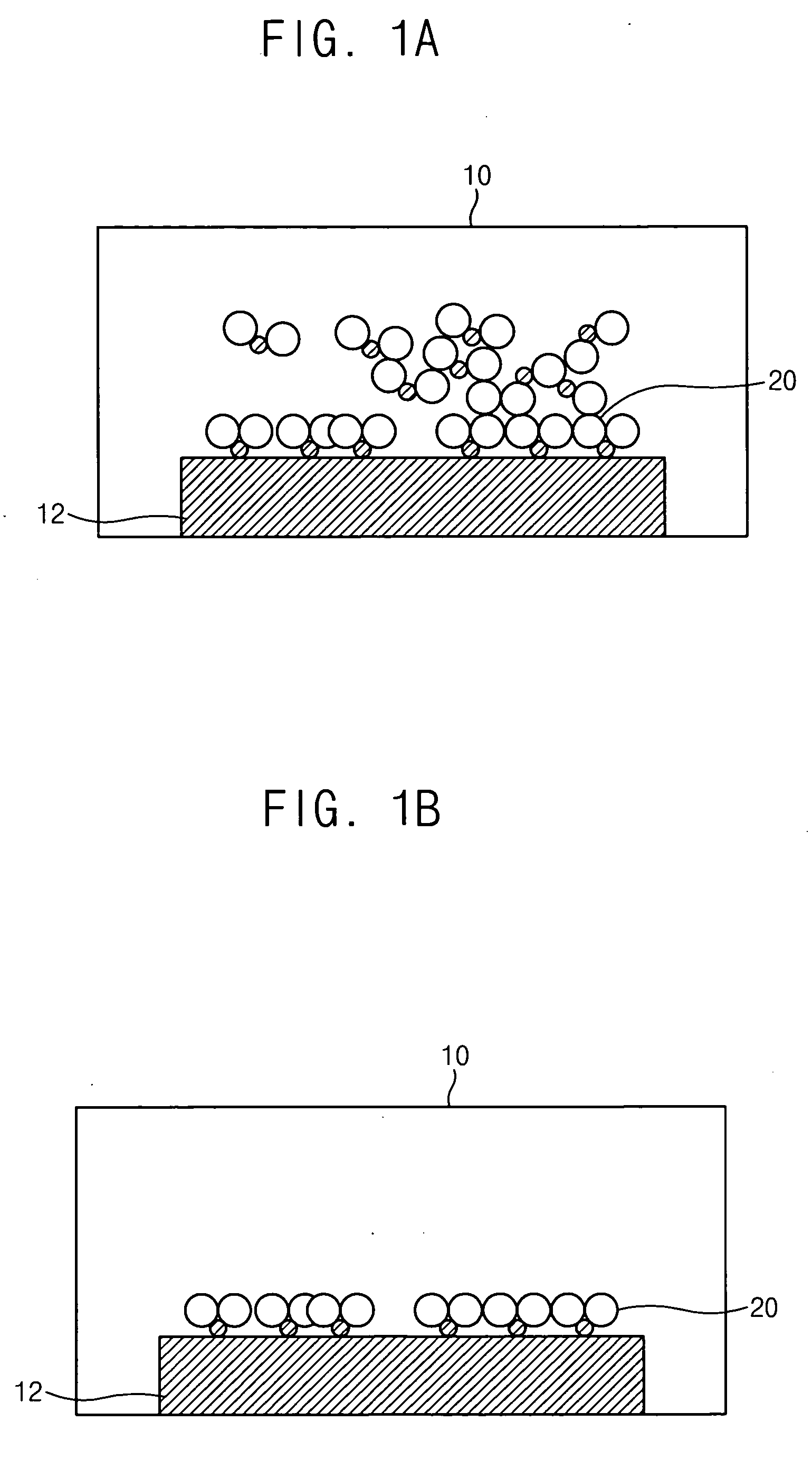
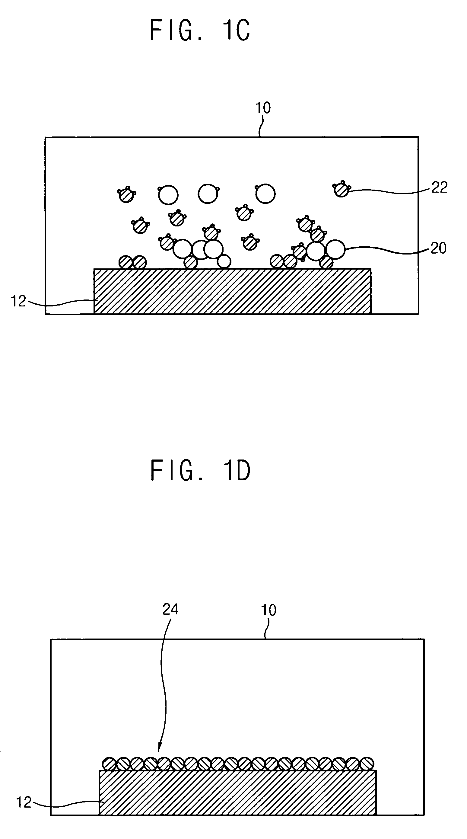
[0043] Exemplary embodiments of the present invention now will be described more fully hereinafter with reference to the accompanying drawings. In the drawings, the thickness of layers and regions are exaggerated for clarity. Like reference numerals refer to similar or identical elements throughout. It will be understood that when an element such as a layer, region or substrate is referred to as being “on” or “onto” another element, it can be directly on the other element or intervening elements may also be present.

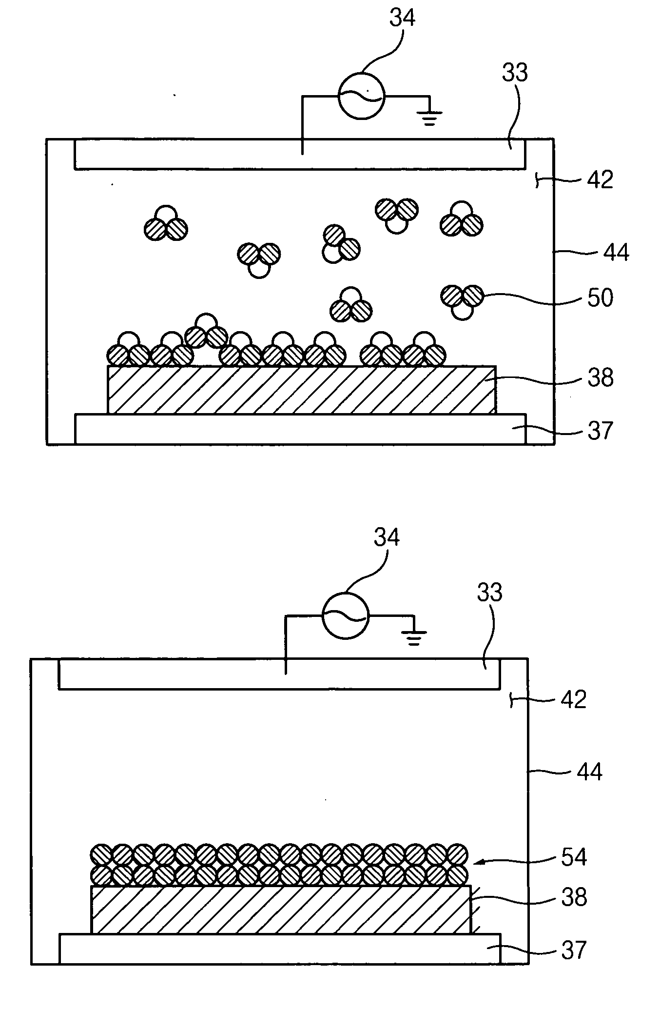
[0044]FIG. 2 is a cross sectional view illustrating an apparatus for forming a layer using an atomic layer deposition (ALD) process in accordance with an exemplary embodiment of the present invention.

[0045] Referring to FIG. 2, the apparatus for forming the layer includes a chamber 44 having a reaction space 42 provided therein.

[0046] A gas inlet 31 is connected to an upper portion of the chamber 44, and a gas supply member 32 is connected to the gas inlet 31. The gas ...


PUM

PropertyMeasurementUnit
Plasma poweraaaaaaaaaa

Abstract

In a method of forming a layer using an atomic layer deposition process, after a substrate is loaded into a chamber, a reactant is provided onto the substrate to form a preliminary layer. Atoms in the preliminary layer are partially removed from the preliminary layer using plasma formed from an inert gas such as an argon gas, a xenon gas or a krypton gas, or an inactive gas such as an oxygen gas, a nitrogen gas or a nitrous oxide gas to form a desired layer. Processes for forming the desired layer may be simplified. A highly integrated semiconductor device having improved reliability may be economically manufactured so that time and costs required for the manufacturing of the semiconductor device may be reduced.

Description

CROSS-REFERENCE TO RELATED APPLICATION [0001] This application claims priority under 35 USC § 119 to Korean Patent Application No. 2004-42551 filed on Jun. 10, 2004, the content of which is incorporated herein by reference in its entirety. BACKGROUND OF THE INVENTION [0002] 1. Field of the Invention [0003] Exemplary embodiments of the present invention relate to methods of forming a layer and methods of forming a capacitor having the layer. More particularly, exemplary embodiments of the present invention relate to methods of forming a layer using an atomic layer deposition (ALD) process and methods of forming a capacitor having the layer. [0004] 2. Description of the Related Art [0005] Since the trend in the art requires semiconductor devices to have high storage capacity and high response speed, semiconductor manufacturing technology has been developed to improve the degree of integration, reliability and response speed of the semiconductor devices. [0006] Dynamic random access me...

Claims


Application Information

Patent Timeline
IPC IPC(8): H01L21/20C23C16/455H01L21/205C23C16/515H01L21/8242
CPCC23C16/45531C23C16/4554C23C16/45553C23C16/515H01L28/65H01L21/31604H01L21/31616H01L21/31691H01L28/40H01L21/3141H01L21/02274H01L21/0228H01L21/205H10B99/00
Inventor LEE, JONG-CHEOLIM, KI-VINKIM, SUNG-TAEKIM, YOUNG-SUNYOO, CHA-YOUNGCHOI, HAN-MEINAM, GAB-JIN
Owner SAMSUNG ELECTRONICS CO LTD
Why Eureka
Try Eureka