Integrated barrier and seed layer for copper interconnect technology

a technology of interconnecting barrier and seed layer, which is applied in the direction of semiconductor devices, semiconductor/solid-state device details, electrical apparatus, etc., can solve the problems of reducing the yield loss of ru, reducing the stress level of the inner layer, and reducing the production cost of tool capital expenditure and yield loss

Active Publication Date: 2006-03-23
BELL SEMICON LLC
View PDF4 Cites 59 Cited by
  • Summary
  • Abstract
  • Description
  • Claims
  • Application Information

AI Technical Summary

Benefits of technology

[0007] The present invention is directed to an integrated barrier and seed layer that is useful for creating conductive pathways in semiconductor devices. The barrier portion of the integrated layer prevents diffusion of the conductive material into the underlying dielectric substrate while the seed portion provides an appropriate foundation upon which to deposit the conductive material. The barrier portion of the integrated layer is formed of a metal ni...

Problems solved by technology

Although a proven technology, the tri-layer deposition of TaN/Ta—Cu does not scale well below 65 mn technology where a high resistance TaN/Ta barrier layer starts to occupy a greater fraction of conductor volume.
In addition, deposition of Cu seed layers typically result in a relatively thick metal layer overhang near the opening of vias and trenches that prevent successful...

Method used


Image

  • Integrated barrier and seed layer for copper interconnect technology
  • Integrated barrier and seed layer for copper interconnect technology
  • Integrated barrier and seed layer for copper interconnect technology

Examples


Embodiment Construction

[0020] The present invention will now be described in detail with reference to a few preferred embodiments thereof as illustrated in the accompanying drawings. In the following description, numerous specific details are set forth in order to provide a thorough understanding of the present invention. It will be apparent, however, to one skilled in the art, that the present invention may be practiced without some or all of these specific details. In other instances, well known operations have not been described in detail so not to unnecessarily obscure the present invention.

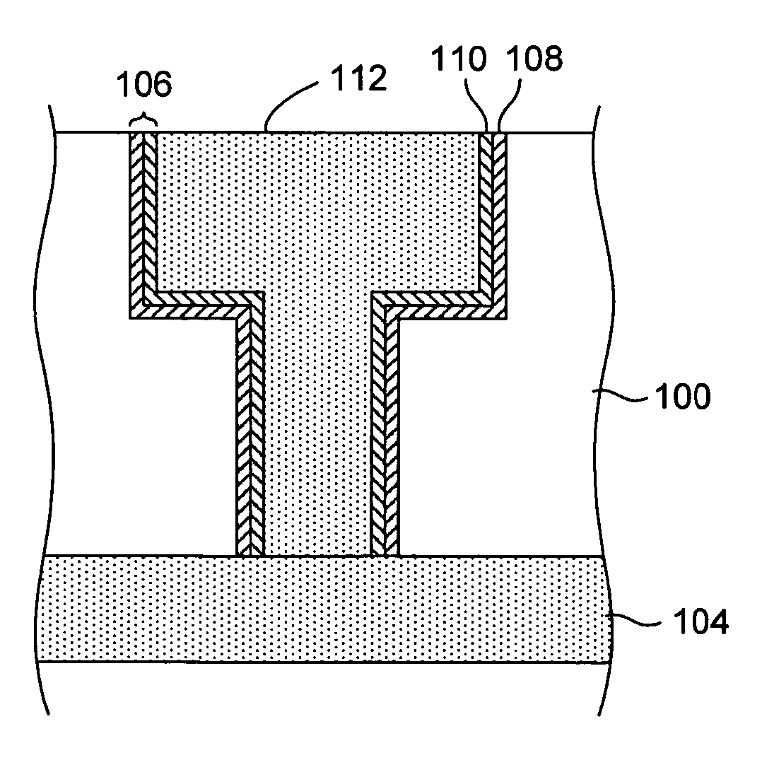
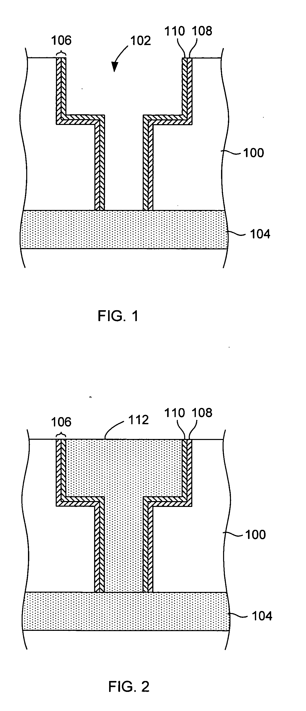
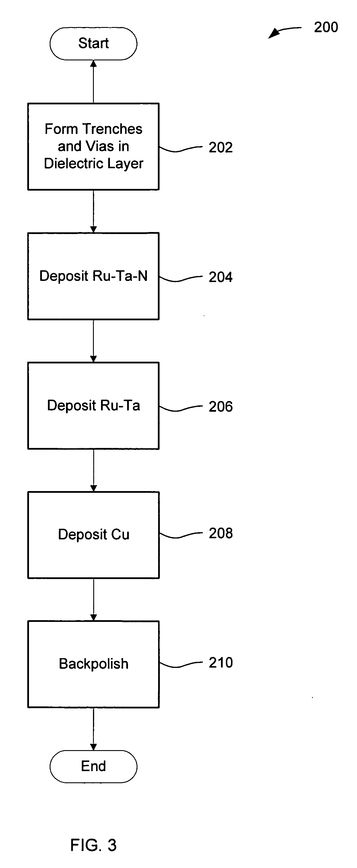
[0021] The present invention pertains to an integrated barrier and seed layer that is useful for creating conductive pathways in semiconductor devices. For example, the integrated barrier and seed layer is formed upon a dielectric substrate so that a conductive material can then be formed upon the integrated barrier and seed layer. The barrier portion of the integrated layer prevents diffusion of the conductive ma...


PUM


Abstract

An integrated barrier and seed layer that is useful for creating conductive pathways in semiconductor devices. The barrier portion of the integrated layer prevents diffusion of the conductive material into the underlying dielectric substrate while the seed portion provides an appropriate foundation upon which to deposit the conductive material. The barrier portion of the integrated layer is formed of a metal nitride, while the seed portion is formed of ruthenium or a ruthenium alloy. The metal nitride forms an effective barrier layer while the ruthenium or ruthenium alloy forms an effective seed layer for a metal such as copper. In some embodiments, the integrated layer is formed in a way so that its composition changes gradually from one region to the next.

Description

FIELD OF THE INVENTION [0001] The present invention relates generally to semiconductor device fabrication, and more specifically to copper interconnect technology. BACKGROUND [0002] Copper interconnect technology has been widely adopted for advanced high performance integrated circuit devices. Because copper (Cu) has a higher melting point than aluminum, it was expected that Cu would have improved current carrying capability and extended electro-migration lifetime. Conventionally, Cu metallization is formed by depositing a thin barrier metal layer, e.g., formed of tantalum-nitrate and tantalum (TaN / Ta), in the trenches or vias formed in dielectric layers by dry etching. A thin Cu metal seed layer then covers the barrier layer. The Cu seed layer is needed for subsequent electroplating of a Cu layer in order to completely fill the vias and trenches of the dielectric layers. Any overplated Cu layers are chemical mechanically polished back to leave Cu metallization in the trenches and v...

Claims


Application Information

Patent Timeline
IPC IPC(8): H01L21/4763
CPCH01L21/76843H01L21/76844H01L23/53238H01L21/76871H01L21/76873H01L21/76846H01L2924/0002H01L2924/00
Inventor SUN, SEY-SHINGKWAK, BYUNG-SUNG L.BURKE, PETER A.
Owner BELL SEMICON LLC
Why Eureka
Try Eureka