Hybrid orientation CMOS with partial insulation process

a technology of partial insulation and hybrid orientation, which is applied in the direction of semiconductors, electrical equipment, semiconductor devices, etc., can solve the problems of significant deformation of electron mobilities on (b>110/b>) si surfaces, inability to adapt to nfet devices, and undesirable pfets with larger widths, etc., to achieve the effect of reducing the junction capacitance, and improving the performance of the devi

Inactive Publication Date: 2006-04-06
GLOBALFOUNDRIES INC
View PDF5 Cites 58 Cited by
  • Summary
  • Abstract
  • Description
  • Claims
  • Application Information

AI Technical Summary

Benefits of technology

[0009] The present invention provides a method of integrating semiconductor devices such that different types of devices are formed upon a specific crystal orientation of a hybrid substrate that enhances the performance of each type of device. Specifically, the present invention provides a method of integrating semiconductor devices such that the pFETs are located on a (110) crystallographic plane, while the nFETs are located on a (100) crystallographic plane of a hybrid substrate. The method of the present invention also improves the performance of the device on an epitaxial semiconductor layer by reducing its junction capacitance using a source / drain diffusion layer on a buried insulator.

Problems solved by technology

To compensate for this discrepancy, pFETs are typically designed with larger widths in order to balance pull-up currents against the nFET pull-down currents and achieve uniform circuit switching. pFETs having larger widths are undesirable since they take up a significant amount of chip area.
Unfortunately, electron mobilities on (110) Si surfaces are significantly degraded compared to (100) Si surfaces.
As can be deduced from the above discussion, the (110) Si surface is optimal for pFET devices because of excellent hole mobility, yet such a crystal orientation is completely inappropriate for nFET devices.
In general, bulk-like devices have larger junction capacitance than SOI devices and will affect circuit performance under AC conditions.
Techniques are known which are capable of fabricating both types of devices on SOI, however the processing steps involved in these prior art techniques are very complicated.

Method used


Image

  • Hybrid orientation CMOS with partial insulation process
  • Hybrid orientation CMOS with partial insulation process
  • Hybrid orientation CMOS with partial insulation process

Examples


Embodiment Construction

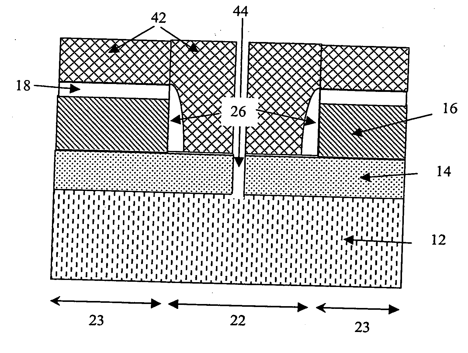
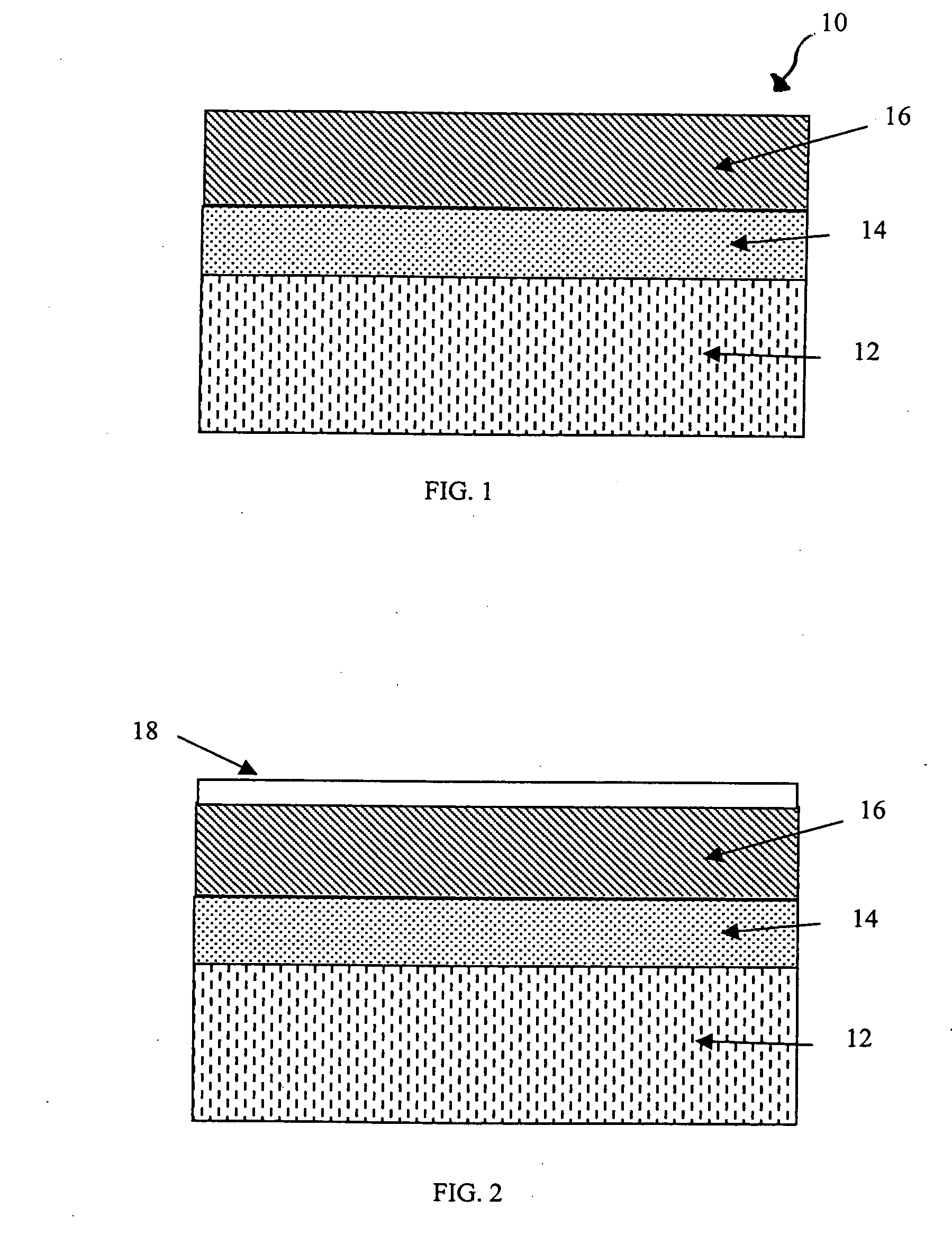
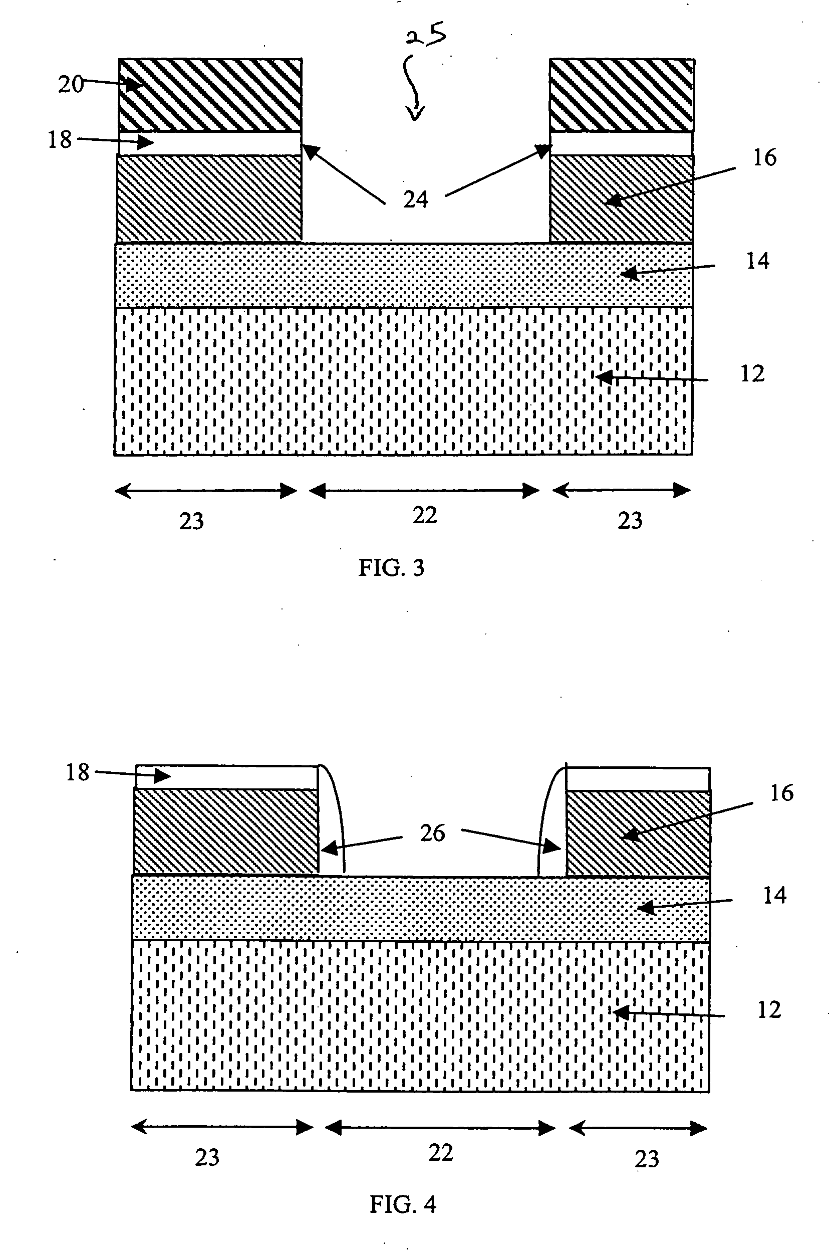
[0033] The present invention, which provides a method of fabricating CMOS devices with reduced junction capacitance on a hybrid substrate having first and second semiconducting layers of different crystal orientations, will now be described in greater detail by referring to the drawings that accompany the present application. It is noted that the drawings provided in the present invention are for illustrative purposes and thus they are not drawn to scale.

[0034] In the drawings, the final hybrid substrate has upper coplanar regions of different crystallographic orientation.

[0035] Referring to FIG. 1, there is shown an initial hybrid substrate 10 that is employed in the present invention. The hybrid substrate 10 comprises a first (or bottom) semiconducting layer 12, a buried insulating layer 14 located on a surface of the first semiconducting layer 12, and a second (or top) semiconducting layer 16 located on a surface of the buried insulating layer 14. In accordance with the present...


PUM


Abstract

The present invention provides a method of integrated semiconductor devices such that different types of devices are formed upon a specific crystallographic orientation of a hybrid substrate. In accordance with the present invention, junction capacitance of one of the devices is improved in the present invention by forming the source / drain diffusion regions of the device in an epitiaxial semiconductor material such that they are situated on a buried insulating layer that extends partially underneath the body of the second semiconductor device. The second semiconductor device, together with the first semiconductor device, is both located atop the buried insulating layer. Unlike the first semiconductor device in which the body thereof is floating, the second semiconductor device is not floating. Rather, it is in contact with an underlying first semiconducting layer.

Description

FIELD OF THE INVENTION [0001] The present invention relates to high-performance metal oxide semiconductor field effect transistors (MOSFETs) for digital or analog applications, and more particularly to MOSFETs utilizing carrier mobility enhancement from surface orientation. BACKGROUND OF THE INVENTION [0002] In present semiconductor technology, complementary metal oxide semiconductor (CMOS) devices, such as nFETs or pFETs, are typically fabricated upon semiconductor wafers, such as Si, that have a single crystal orientation. In particular, most of today's semiconductor devices are built upon Si having a (100) crystal orientation. [0003] Electrons are known to have a high mobility for a (100) Si surface orientation, but holes are known to have high mobility for a (110) surface orientation. That is, hole mobility values on (100) Si are roughly 2×-4× lower than the corresponding electron mobility for this crystallographic orientation. To compensate for this discrepancy, pFETs are typic...

Claims


Application Information

Patent Timeline
Patent Type & Authority Applications(United States)
IPC IPC(8): H01L21/84H01L21/20H01L21/8238
CPCH01L21/84H01L27/1207H01L27/1203
Inventor YANG, MIN
Owner GLOBALFOUNDRIES INC
Why Eureka
Try Eureka