Selective etching processes of silicon nitride and indium oxide thin films for FeRAM device applications

a technology of indium oxide and etching process, which is applied in the direction of semiconductor/solid-state device details, transistors, solid-state devices, etc., can solve the problem that the etch rate of silicon oxide cannot be reduced with the addition, and achieve the effect of preventing degradation of ferroelectric materials and minimizing the damage of conductive oxid

Inactive Publication Date: 2006-04-06
SHARP KK
View PDF23 Cites 37 Cited by
  • Summary
  • Abstract
  • Description
  • Claims
  • Application Information

AI Technical Summary

Benefits of technology

[0009] The present invention selective etching of Si3N4 over conductive oxide such as In2O3 can be applicable for silicon nitride spacer formation on a surface of In2O3 layer to minimize the overetched damage to the conducti

Problems solved by technology

However, etch selective improvement of silicon oxide with oxygen additive is credited to the reduction of

Method used


Image

  • Selective etching processes of silicon nitride and indium oxide thin films for FeRAM device applications
  • Selective etching processes of silicon nitride and indium oxide thin films for FeRAM device applications
  • Selective etching processes of silicon nitride and indium oxide thin films for FeRAM device applications

Examples


Embodiment Construction

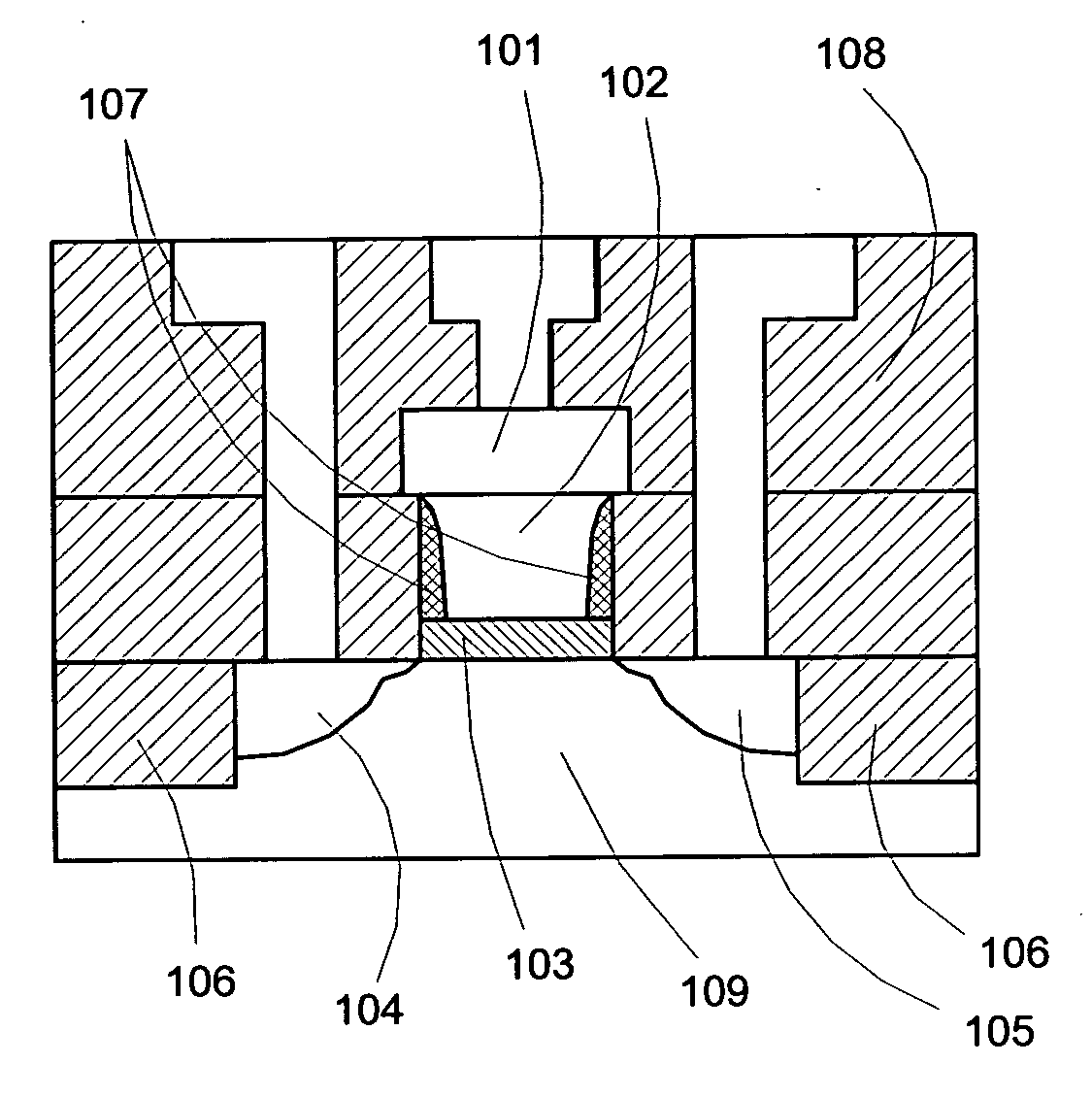
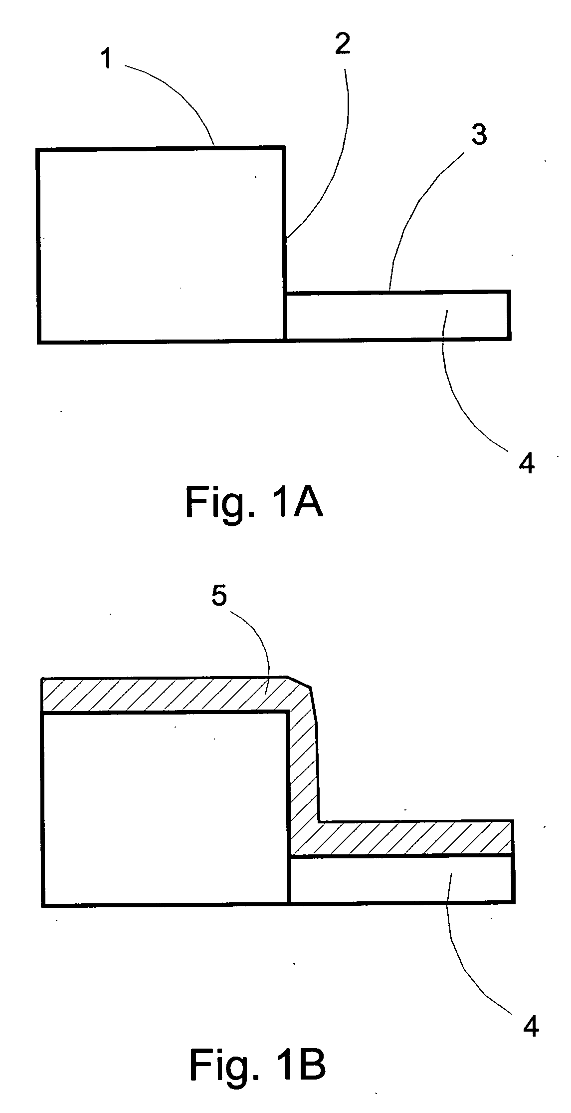
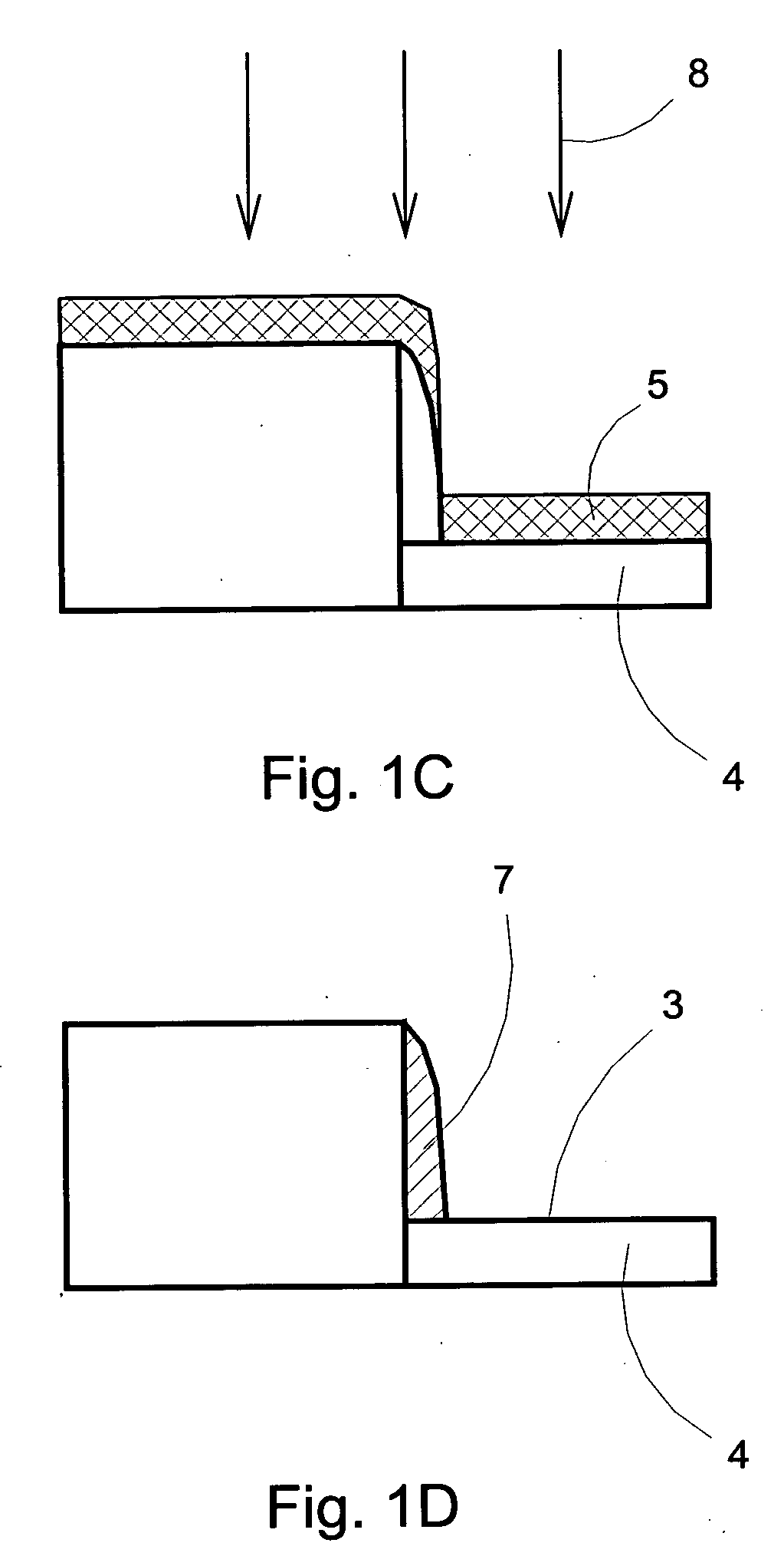
[0014] The present invention discloses a selective etch process between silicon nitride and conductive oxide materials, applicable for the fabrication of semiconductor devices, especially for ferroelectric memory transistors employing conductive oxide. Using the present invention etch selectivity method, silicon nitride spacers encapsulated the ferroelectric material can be fabricated with less damage to the conductive oxide layer. The conductive oxide used in the present invention is broadly defined as an oxide that is not a dielectric, including conductive metal oxide, doped conductive oxide, doped conductive metal oxide, semiconductive oxide and semiconductive metal oxide materials.

[0015] Briefly, the present invention comprises an etch gas mixture having an oxygen additive wherein the oxygen comprises between 1-15% by volume of the etch gas mixture. The etch gas mixture typically contains chlorine or fluorine compound such as C4F8, CF4, C2F6, CHF3, C3F6, C4F6, C5F8, Cl2, CF2Cl2...


PUM

PropertyMeasurementUnit
Fractionaaaaaaaaaa
Pressureaaaaaaaaaa
Poweraaaaaaaaaa

Abstract

A dry etch process is described for selectively etching silicon nitride from conductive oxide material for use in a semiconductor fabrication process. Adding an oxidant in the etch gas mixture could increase the etch rate for the silicon nitride while reducing the etch rate for the conductive oxide, resulting in improving etch selectivity. The disclosed selective etch process is well suited for ferroelectric memory device fabrication using conductive oxide/ferroelectric interface having silicon nitride as the encapsulated material for the ferroelectric.

Description

FIELD OF THE INVENTION [0001] This invention relates in general to selective etching of silicon nitride relative to conductive oxide, and particularly to improved methods for integrated processes of ferroelectric non-volatile memory devices. BACKGROUND OF THE INVENTION [0002] Ferroelectric materials are composed of many randomly-distributed permanently polarized regions. Under the presence of an electric field, the regions with a polarization component in the direction of the electric field grow at the expense of the non-aligned regions so that a net polarization can result. If the electric field decreases, the polarization also decreases but at a slower rate so that even when the electric field becomes zero, a remnant polarization remains. This remnant polarization, existed under zero field condition (i.e., when power is turned off), is the basis of ferroelectric nonvolatile memory devices such as ferroelectric transistors. [0003] The ferroelectric transistor is typically a ferroel...

Claims


Application Information

Patent Timeline
IPC IPC(8): H01L21/302
CPCH01L21/31116H01L29/6684H01L29/78391
Inventor LI, TINGKAIHSU, SHENG TENGULRICH, BRUCE D.BURGHOLZER, MARK A.HILL, RAY A.
Owner SHARP KK
Why Eureka
Try Eureka