Gallium-nitride based light-emitting diodes structure with high reverse withstanding voltage and anti-ESD capability

a technology of gallium nitride and light-emitting diodes, which is applied in the direction of basic electric elements, electrical equipment, semiconductor devices, etc., can solve the problems of complex flip-chip process, inferior epitaxial quality of gan-based leds,

Inactive Publication Date: 2006-04-13
FORMOSA EPITAXY INCORPORATION
View PDF11 Cites 18 Cited by
  • Summary
  • Abstract
  • Description
  • Claims
  • Application Information

AI Technical Summary

Benefits of technology

[0010] The present invention provides an epitaxial structure for the GaN-based LEDs so that the limitations and disadvantages in terms of their anti-ESD capability from the prior arts can be obviated practically.

Problems solved by technology

GaN-based nitrides and the sapphire substrate usually have mismatched lattice constants, causing an excessive accumulation of stresses and, thereby, causing the GaN-based LEDs to have an inferior epitaxial quality.
Although this solution indeed effectively improves the GaN-based LED's anti-ESD capability, the flip-chip process is much more complicated than the traditional manufacturing process for general GaN-based LEDs.

Method used


Image

  • Gallium-nitride based light-emitting diodes structure with high reverse withstanding voltage and anti-ESD capability
  • Gallium-nitride based light-emitting diodes structure with high reverse withstanding voltage and anti-ESD capability
  • Gallium-nitride based light-emitting diodes structure with high reverse withstanding voltage and anti-ESD capability

Examples


first embodiment

[0020]FIG. 2 is a schematic diagram showing a GaN-based LED device according to the present invention. As shown in FIG. 2, the GaN-based LED device has a substrate 10 made of C-plane, R-plane, or A-plane aluminum-oxide monocrystalline (sapphire), or an oxide monocrystalline having a lattice constant compatible with that of nitride semiconductors. The substrate 10 can also be made of SiC (6H-SiC or 4H-SiC), Si, ZnO, GaAs, or MgAl2O4. Generally, the most common material used for the substrate 10 is sapphire or SiC. An optional buffer layer 20 made of a GaN-based material whose molecular formula could be expressed as AlaGabIn1-a-bN (0≦a,b10. On top of the buffer layer 20, a first contact layer 30 is formed and made of a GaN-based material having a first conduction type (e.g., it could a p-typed GaN or n-typed GaN). Then, on top of the first contact layer 30, an active layer 40 made of a GaN-based material such as InGaN is formed on top of the first contact layer 30.

[0021] On top of the...

second embodiment

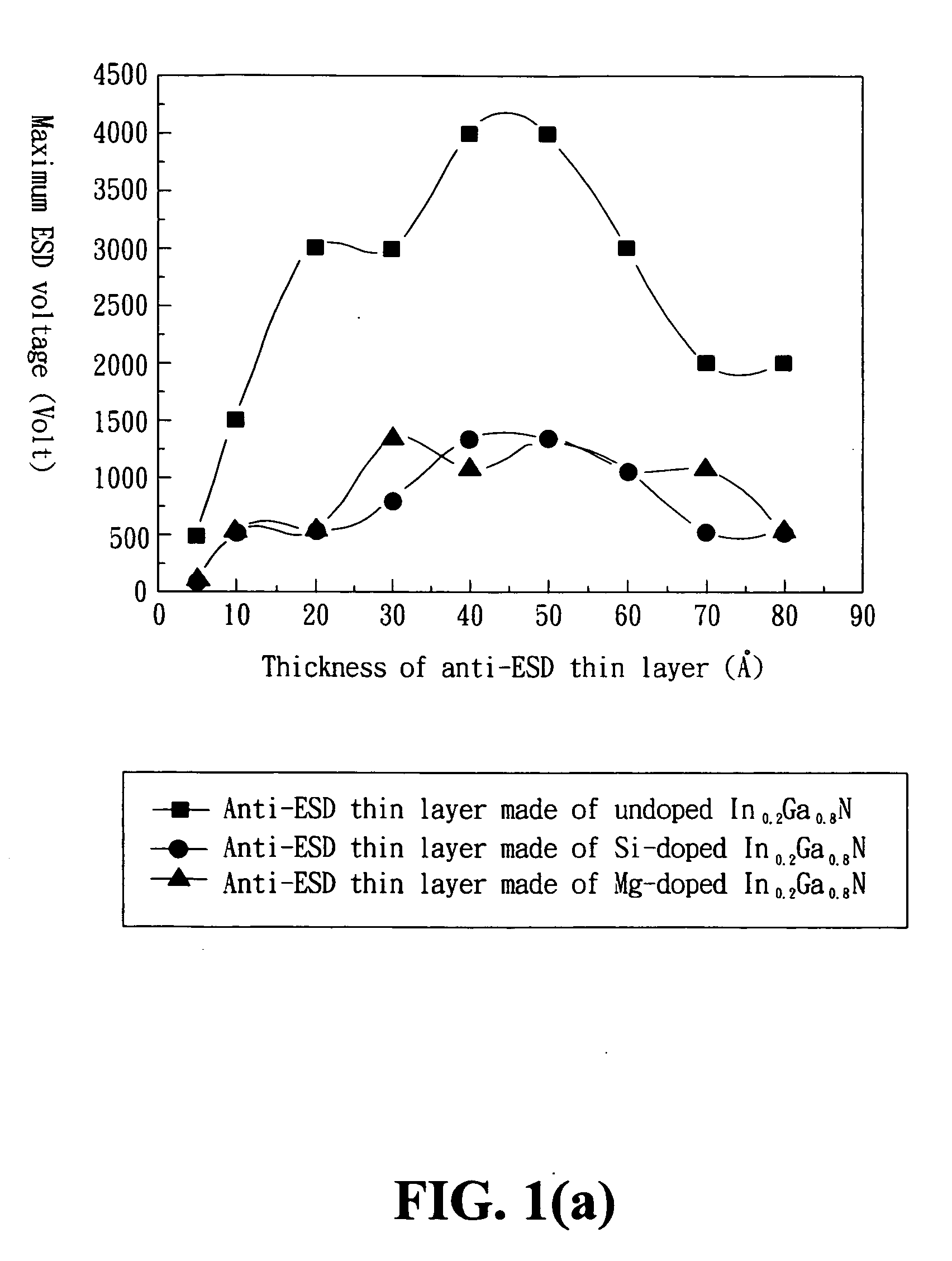
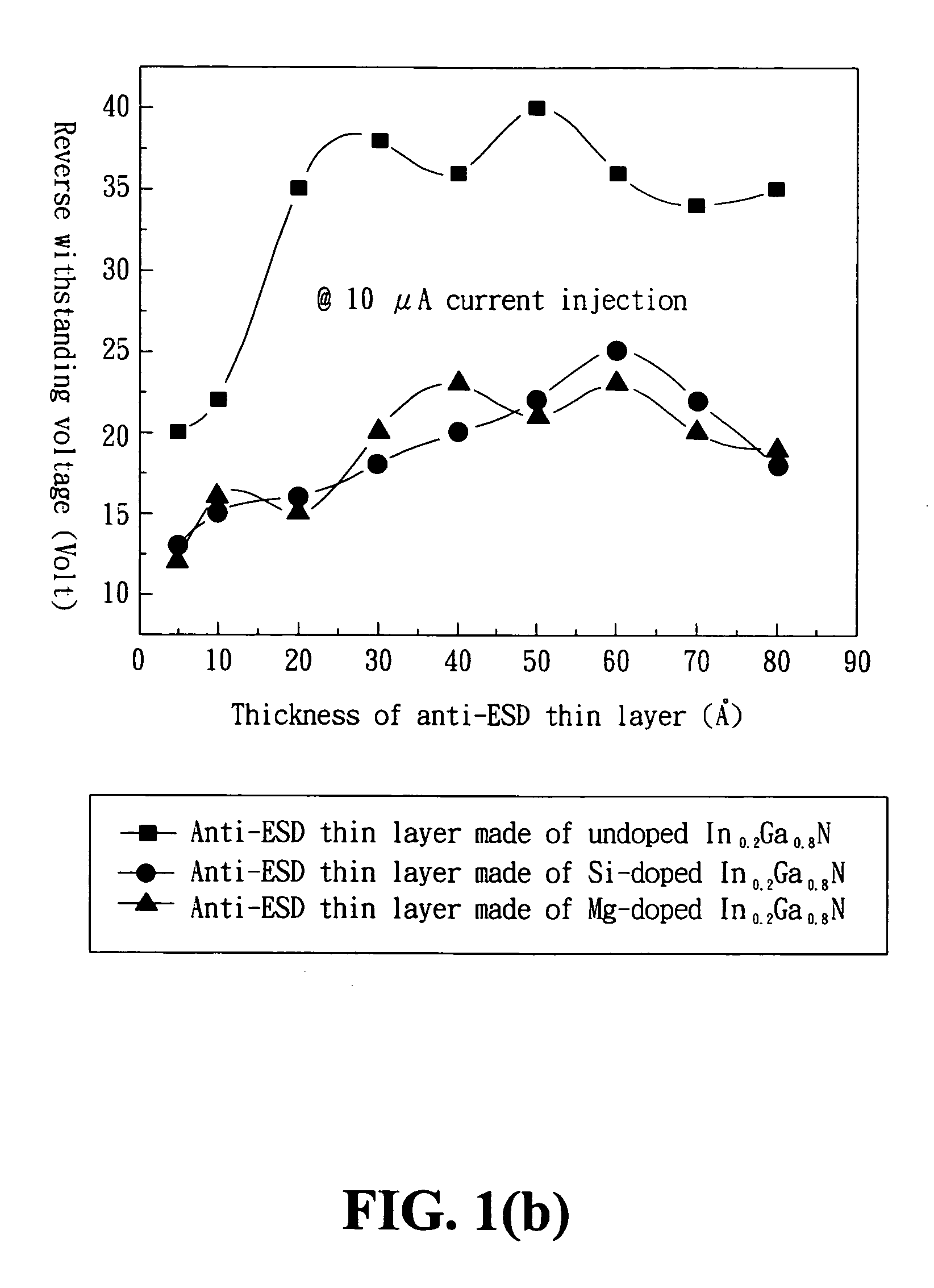
[0024]FIG. 3 is a schematic diagram showing a GaN-based LED device according to the present invention. As shown in FIG. 3, this embodiment of the present invention has an identical structure as in the previous embodiment. The only difference lies in the material used for the anti-ESD thin layer. In this embodiment, the anti-ESD thin layer 72 is made of undoped, low-band-gap (EgeInfGa1-e-fN (072 has a thickness between 5 Å and 100 Å and a growing temperature between 600° C. and 1100° C.

third embodiment

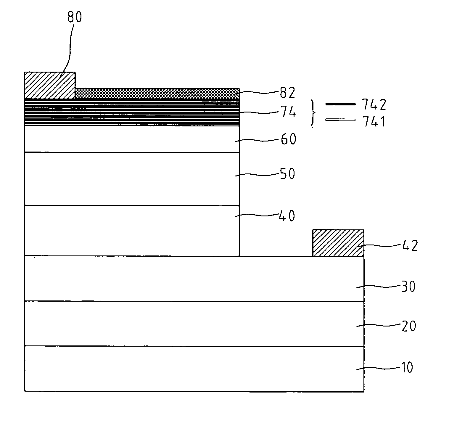
[0025]FIG. 4 is a schematic diagram showing a GaN-based LED according to the present invention. As shown in FIG. 4, this embodiment of the present invention has an identical structure as in the previous embodiments. The only difference lies in the material used and the structure of the anti-ESD thin layer. In this embodiment, the anti-ESD thin layer 74 has a superlattice structure formed by interleaving one or more InGaN thin layers 741 with one or more AlInGaN thin layers 742. Each of the InGaN thin layers 741 is made of undoped IngGa1-gN (0gGa1-gN composition (i.e. the parameter g of the foregoing molecular formula) of each InGaN thin layer 741 is not required to be identical. On the other hand, each of the AlInGaN thin layers 742 is made of undoped, low-band-gap (EghIniGa1-h-iN (0hIniGa1-h-iN composition (i.e. the parameters h and i of the foregoing molecular formula) of each AlInGaN thin layer 742 is not required to be identical.

[0026] Within the anti-ESD thin layer 74's superla...


PUM


Abstract

An epitaxial structure for GaN-based LEDs to achieve better reverse withstanding voltage and anti-ESD capability is provided herein. The epitaxial structure has an additional anti-ESD thin layer as the topmost layer, which is made of undoped indium-gallium-nitrides (InGaN) or low-band-gap (Eg<3.4 eV), undoped aluminum-indium-gallium-nitrides (AlInGaN). The anti-ESD thin layer could also have a superlattice structure formed by interleaving at least an undoped InGaN thin layer and at least a low-band-gap, undoped AlInGaN thin layer. This anti-ESD thin layer greatly improves the GaN-based LEDs' reverse withstanding voltage and resistivity to ESD, which in turn extends the GaN-based LEDs' operation life significantly.

Description

CROSS-REFERENCE TO RELATED APPLICATIONS [0001] This is a continuation-in-part of U.S. application Ser. No. 10 / 964,350, filed on Oct. 12, 2004.BACKGROUND OF THE INVENTION [0002] 1. Field of the Invention [0003] The present invention generally relates to the gallium-nitride based light-emitting diodes and, more particularly, to an epitaxial structure of the gallium-nitride based light-emitting diodes having a high reverse withstanding voltage and a high resistivity to electrostatic discharge. [0004] 2. The Prior Arts [0005] Gallium-nitride (GaN) based light-emitting diodes (LEDs), as various color LEDs can be developed by controlling the GaN-based material's composition, has been the research and development focus in the academic arena and in the industries as well in recent years. Besides being applied in the display of consumer electronic appliances such as digital clocks and cellular handsets, technology breakthroughs in terms of luminance and lighting efficiency has led GaN-based ...

Claims


Application Information

Patent Timeline
Patent Type & Authority Applications(United States)
IPC IPC(8): H01L33/00H01L33/02H01L33/04H01L33/32
CPCH01L27/15H01L33/02H01L33/04H01L33/32
Inventor WU, LIANG-WENCHIEN, FEN-REN
Owner FORMOSA EPITAXY INCORPORATION
Why Eureka
Try Eureka