Semiconductor device manufacturing method

Inactive Publication Date: 2006-04-13
LAPIS SEMICON CO LTD
View PDF9 Cites 9 Cited by
  • Summary
  • Abstract
  • Description
  • Claims
  • Application Information

AI Technical Summary

Benefits of technology

[0011] The silicon oxynitride film (i.e., MOSFET gate insulation film) is very thin, but entry of nitrogen into the interface between the

Problems solved by technology

The uneven distribution of nitrogen causes major dete

Method used


Image

  • Semiconductor device manufacturing method
  • Semiconductor device manufacturing method
  • Semiconductor device manufacturing method

Examples


first embodiment

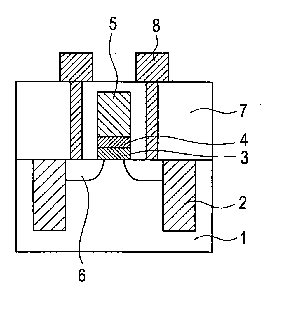
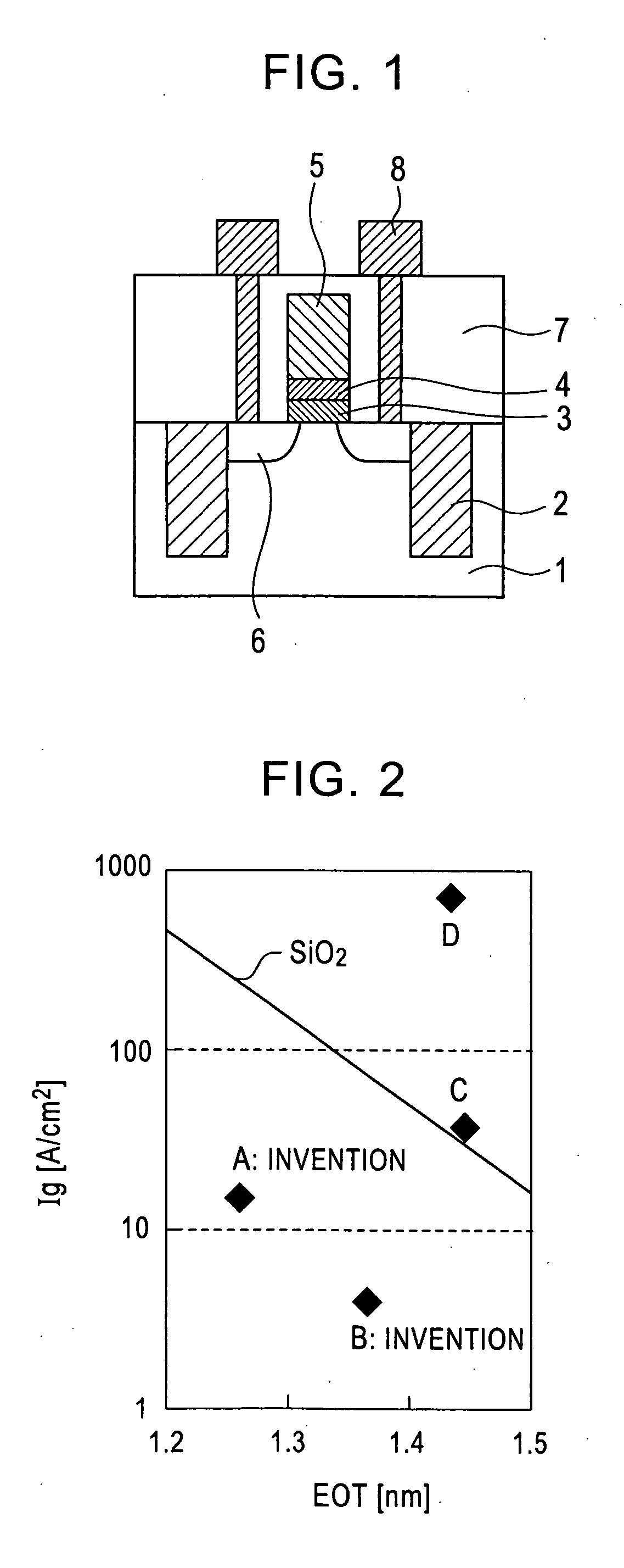
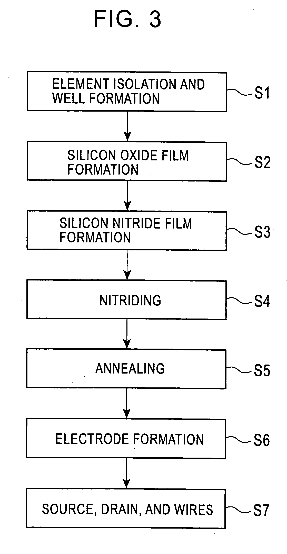
[0017] Referring to FIG. 1 and FIG. 3, the isolated elements 2 are formed on the semiconductor substrate 1 with a known method (STI in this embodiment) (Step S1 in FIG. 3). Then, wells and channels are formed with the ion implantation method (not shown in FIG. 1) (Step S1 in FIG. 3). STI stands for shallow trench isolation.

[0018] Next, the silicon oxide film 3 is formed to a thickness of between 0.5 nm and 1.5 nm over the entire surface (Step S2). The silicon oxide film is formed using the thermal oxidation method or plasma oxidation method or any other suitable method.

[0019] Next, the silicon nitride film 4 is formed to a thickness of between 0.2 nm and 1 nm using the LPCVD (Low Pressure Chemical Vapor Deposition) method (Step S3). Since formation of an extremely thin film is necessary in the LPCVD method, it is preferred that the ALD (Atomic Layer Deposition) method is used together with the LPCVD method.

[0020] Next, the silicon nitride film 4 is nitrided using the plasma nitri...

second embodiment

[0028] The second embodiment is described with reference to FIG. 1 and FIG. 4. FIG. 4 shows the flowchart to form the MOS transistor. The second embodiment is similar to the first embodiment so that only the differences are described below.

[0029] Steps S21 to S23 in FIG. 4 (second embodiment) are similar to steps S1 to S3 in FIG. 3 (first embodiment).

[0030] After the silicon nitride film 4 is formed (Step S23), annealing is performed in an inert gas atmosphere at a temperature of between 900° C. and 1100° C. for between 1 and 100 seconds (Step S24). Nitriding is then performed (Step S25), and again the annealing is performed in an inert gas atmosphere at a temperature of between 900° C. and 1100° C. for between 1 and 100 seconds (Step S26).

[0031] Next, the gate electrode 5 is formed by diffusing an impurity in polysilicon, and patterning (Step S27).

[0032] Next, using a known method, the source and drain 6 are formed using the ion implantation method, and the interlaminar film 7 ...


PUM


Abstract

A manufacturing method for semiconductor devices having MOSFET gate insulation films. The method includes forming a silicon oxide film, forming a silicon nitride film, nitriding the silicon nitride film, and heat treatment.

Description

BACKGROUND OF THE INVENTION [0001] 1. Field of the Invention [0002] The present invention relates to a manufacturing method for semiconductor devices such as MOSFETs, and more particularly to a manufacturing method for semiconductor devices employing improved gate insulation film formation. [0003] 2. Description of the Related Art [0004] The gate insulation films of MOSFETs have become thinner as semiconductor elements and devices become ever more microscopic. A silicon oxynitride film in which nitrogen has been introduced to control diffusion of boron in the silicon substrate is used in gate insulation films of surface channel type PMOS-FETs having boron-diffused gate electrodes. This silicon oxynitride film is formed primarily by nitriding a silicon oxide film with heat treatment in an atmosphere of N2O, NO, or NH3. [0005] However, nitrogen in the silicon oxynitride film is not evenly distributed in the gate insulation film and the silicon substrate. This deteriorates the device c...

Claims


Application Information

Patent Timeline
IPC IPC(8): H01L21/469
CPCH01L21/28185H01L21/28202H01L29/513
Inventor TAKAHASHI, MASASHI
Owner LAPIS SEMICON CO LTD
Why Eureka
Try Eureka