[0009] An object of the present invention is to provide a substrate processing method and a substrate processing apparatus, which permit improving the peeling rate of, for example, the resist film without
plasma ashing.
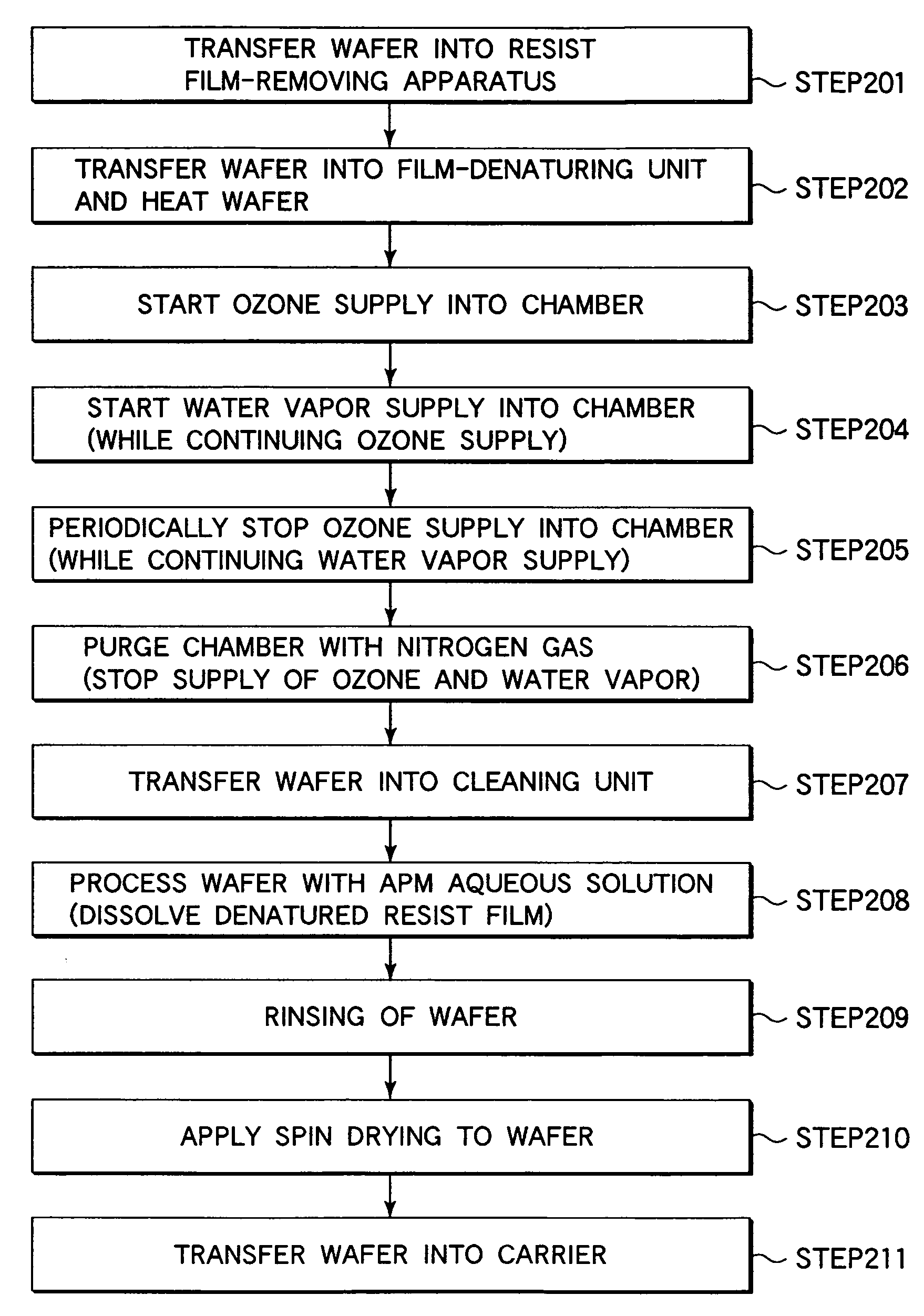
[0011] According to a first aspect of the present invention, there is provided a substrate processing method for removing a resist film from the substrate having the resist film formed thereon, comprising maintaining an inner region of a chamber housing a substrate having a resist film formed thereon at a prescribed temperature, denaturing the resist film by supplying ozone and a water vapor in such a manner that ozone is supplied into the chamber while a water vapor is supplied into the chamber at a prescribed flow rate, the amount of ozone relative to the amount of the water vapor being adjusted such that the
dew formation within the chamber is prevented, and processing the substrate with a prescribed liquid material so as to remove the denatured resist film from the substrate.
[0012] In the substrate processing method of the present invention outlined above, a pure water or an alkaline
aqueous solution is suitably used in removing the denatured resist film from the substrate in the case where a resist film adapted for the KrF line is used as the resist film. Where a resist film adapted for the KrF line, which is formed together with an antireflection film (BARC), is used as the resist film, it is desirable to use an alkaline
aqueous solution in the step of removing the denatured resist film from the substrate. In this case, the antireflection film can be removed more easily. On the other hand, where a resist film adapted for the ArF line is used as the resist film, an alkaline
aqueous solution is suitably used in removing the denatured resist film from the substrate. In general, an antireflection film is formed together with the resist film adapted for the ArF line. In the substrate processing method of the present invention, it is possible to denature the antireflection film in denaturing the resist film such that the antireflection film can be removed by the processing with an alkaline aqueous solution. The alkaline aqueous solution used for removing the denatured resist film from the substrate includes, for example, an APM aqueous solution, an aqueous solution of
ammonium hydroxide, and an aqueous solution of tetramethyl
ammonium hydroxide (TMAH). Particularly, where the metal is exposed to the processing surface of the substrate, it is possible to prevent the metal from being damaged by using any of an aqueous solution of
ammonium hydroxide or an aqueous solution of TMAH.
[0016] According to a fourth aspect of the present invention, there is provided a
computer program containing a
software which, when executed, causes a computer to control a substrate processing apparatus in which a substrate housed in a chamber is processed with a water vapor and ozone, the
software causing the computer to execute a process which comprises maintaining an inner region of the chamber housing a substrate having a resist film formed thereon at a prescribed temperature, denaturing the resist film by supplying ozone and a water vapor in such a manner that ozone is supplied into the chamber housing the substrate at a prescribed temperature while a water vapor is supplied into the chamber at a prescribed flow rate, the amount of ozone relative to the amount of the water vapor being adjusted such that a
dew formation within the chamber is prevented.
[0017] According to a fifth aspect of the present invention, there is provided a
computer program containing a
software which, when executed, causes a computer to control a substrate processing apparatus, the software causing the computer to execute a substrate processing method to remove a resist film from the substrate comprising maintaining an inner region of the chamber housing a substrate having a resist film formed thereon at a prescribed temperature, denaturing the resist film by supplying ozone and a water vapor in such a manner that ozone is supplied into the chamber while a water vapor is supplied into the chamber at a prescribed flow rate, the amount of ozone relative to the amount of the water vapor being adjusted such that the dew formation within the chamber is prevented, and processing the substrate with a prescribed liquid material so as to remove the denatured resist film from the substrate.
[0018] According to a sixth aspect of the present invention, there is provided a storage medium that can be read by a computer, the storage medium containing a software which, when executed, causes a computer to control the substrate processing apparatus, the software causing the computer to execute a substrate processing method to remove a resist film from the substrate comprising maintaining an inner region of the chamber having a substrate having a resist film formed thereon at a prescribed temperature, denaturing the resist film by supplying ozone and a water vapor in such a manner that ozone is supplied into the chamber while a water vapor is supplied into the chamber at a prescribed flow rate, the amount of ozone relative to the amount of the water vapor being adjusted such that the dew formation within the chamber is prevented, and processing the substrate with a prescribed liquid material so as to remove the denatured resist film from the substrate.

