Semiconductor device and manufacturing method of the same
a semiconductor and semiconductor chip technology, applied in semiconductor devices, traveling carriers, travelling articles, etc., can solve the problems of reducing the power ic, and reducing the area of the ic chip, so as to prevent the short channel effect and improve the drain breakdown voltage during operation.
- Summary
- Abstract
- Description
- Claims
- Application Information
AI Technical Summary
Benefits of technology
Problems solved by technology
Method used
Image
Examples
first embodiment
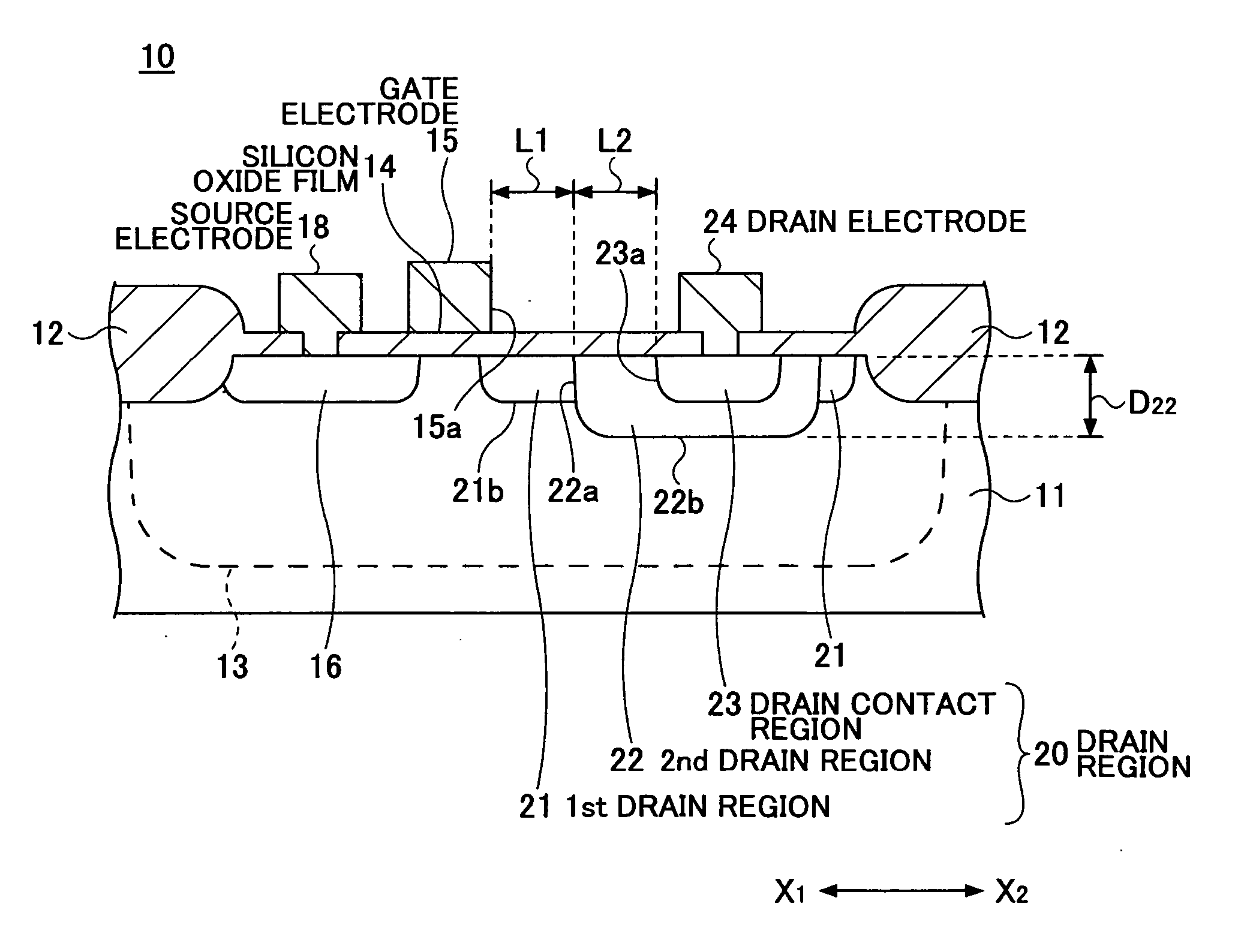
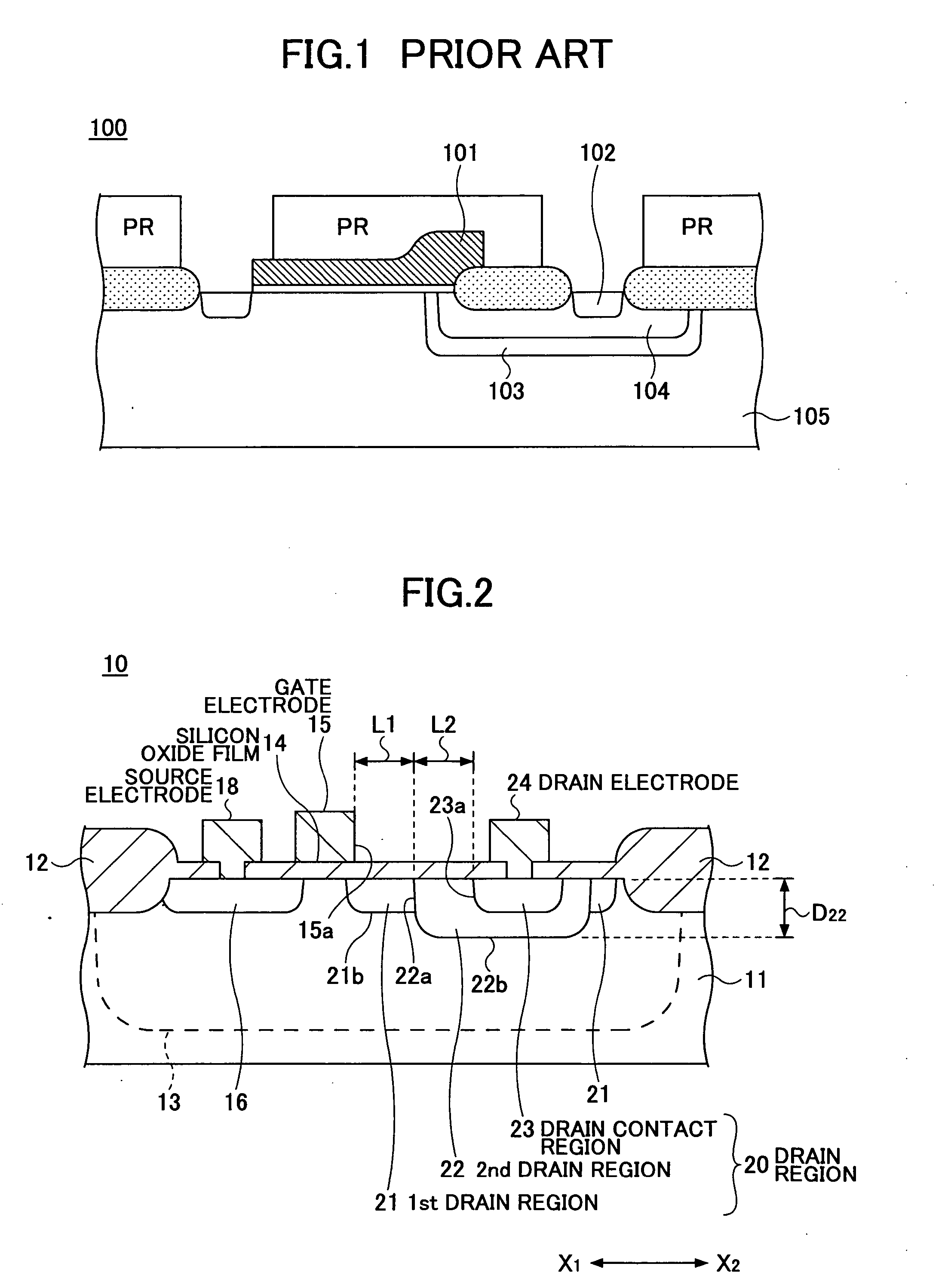
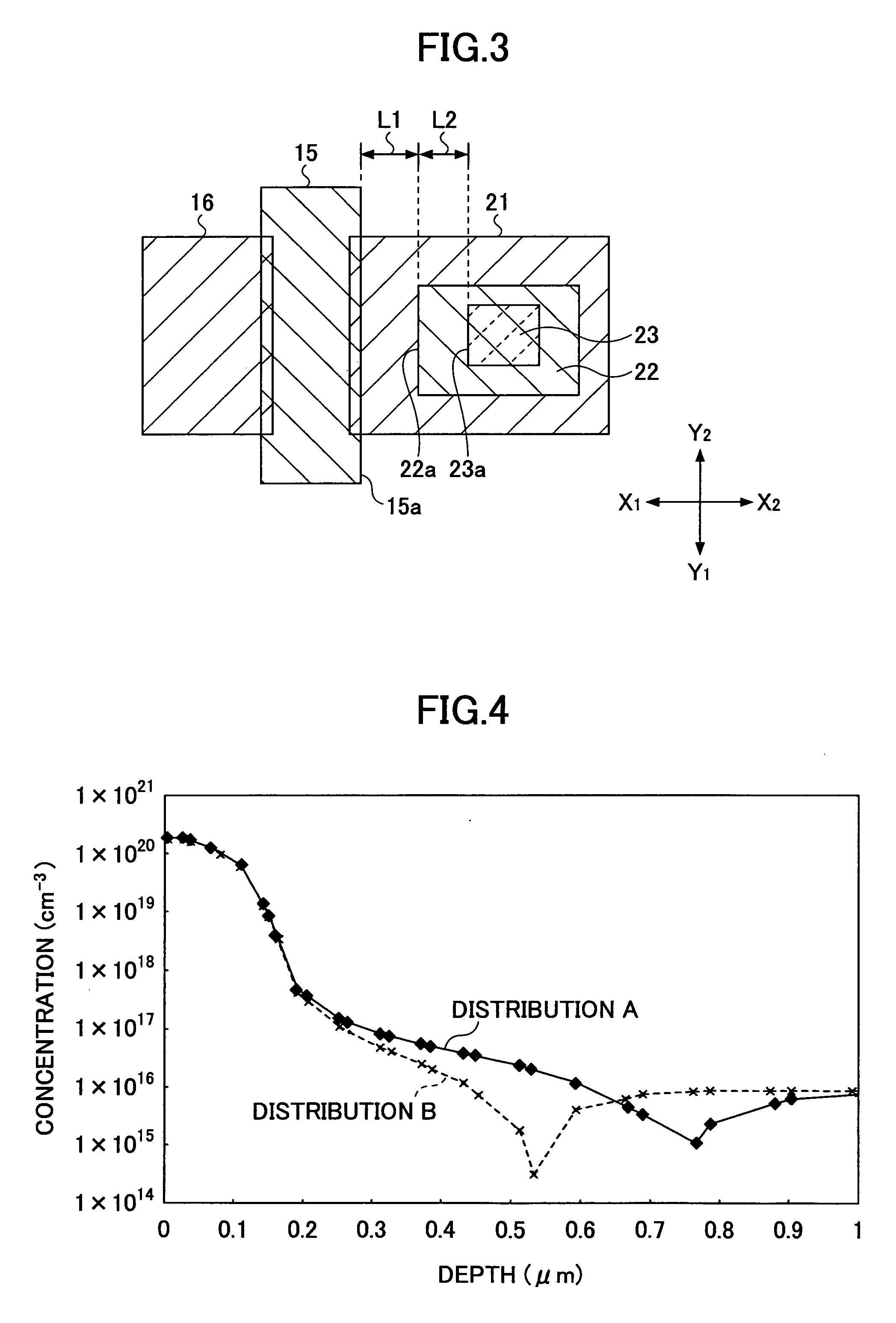
[0050]FIG. 2 is a diagram showing a configuration of a semiconductor device according to a first embodiment of the present invention. FIG. 3 is an exemplary plan view of the semiconductor device according to the first embodiment. It is noted that in the example described below, it is assumed that the semiconductor device corresponds to an n-channel MOS transistor.
[0051] According to the illustrated example of FIGS. 2 and 3, the semiconductor device 10 includes a silicon substrate 11, an isolation region 12, a p-well region 13 that is implanted in the activated region formed by the silicon substrate 11 and the isolation region 12, a silicon oxide film 14 that is formed on the silicon substrate 11 surface as a gate insulating film, a gate electrode 15 that is formed on the silicon oxide film 14, a source region 16 formed on one side of the gate electrode 15, a source electrode 18 that is in contact with the source region 16, a drain region 20 that is formed on the other side of the g...
second embodiment
[0088]FIG. 9 is a cross-sectional diagram showing a configuration of a semiconductor device according to a second embodiment of the present invention. It is noted that in this drawing, elements that are identical to those shown in relation to the first embodiment are assigned the same numerical references, and their descriptions are omitted.
[0089] The semiconductor device 40 according to the second embodiment as is shown in FIG. 9 may correspond to an LD (Laterally Diffused) MOS transistor that includes a silicon substrate 11, an isolation region 12, a p-well region that is arranged at an activated region formed by the isolation region 12, a silicon oxide film 14 that is formed on the surface of the silicon substrate 11 as a gate insulating film, a field oxide film 12a that is continuous with the silicon oxide film 14 and is positioned toward the drain electrode side, a gate electrode 15 that is formed over portions of the silicon oxide film 14 and the field oxide film 12a, a p-wel...
third embodiment
[0093]FIG. 10 is a diagram showing a semiconductor device according to a third embodiment of the present invention. It is noted that in this drawing, elements that are identical to those described in relation to the previous embodiments are assigned the same numerical references and their descriptions are omitted.
[0094] The semiconductor device 50 shown in FIG. 10 includes an offset n-channel MOS transistor 10, an npn bipolar transistor 60, an n-channel MOS transistor 70, and a p-channel MOS transistor 80.
[0095] The npn bipolar transistor 60 includes a base, an emitter, and a collector that is provided in an element region formed by a silicon substrate 11 and an isolation region 12.
[0096] The emitter includes, an n-well region 61, an n-type emitter 62 that is formed inside a p-type base region 63 provided at a surface layer of the silicon substrate 11 within the n-well region 61, and an emitter electrode 67 that is connected to the emitter region 62 via a contact hole that is for...
PUM
 Abstract
Description
Claims
Application Information


