
Catadioptric projection objective with an in-line, single-axis configuration

a technology of in-line, single-axis configuration and catadioptric projection, which is applied in the field of catadioptric projection objective for microlithographic exposure apparatus, can solve the problems of limited selection of materials for lenses in microlithographic objectives, limited design flexibility, and inability to meet the requirements of chromatic aberration correction

Inactive Publication Date: 2006-04-20
CARL ZEISS SMT GMBH
View PDF1 Cites 47 Cited by
  • Summary
  • Abstract
  • Description
  • Claims
  • Application Information

AI Technical Summary

Benefits of technology

The present invention provides a catadioptric microlithographic projection objective for use with ultraviolet light at wavelengths shorter than 260 nm. The objective has a high degree of reflectivity and is designed to direct the light from an object plane to an image plane. The objective includes a first optical subsystem with a plurality of lenses, a second optical subsystem with a concave mirror and a catadioptric lens element, and a third optical subsystem with at least one lens. The objective is designed to provide an image with reduced aberrations and distortions. The invention also includes a beam splitter coating on the second surface of the catadioptric lens element to improve image quality. The technical effects of the invention include improved performance in microlithographic projection and reduced aberrations in the image.

Problems solved by technology

However, only very few lens materials are sufficiently transparent to ultraviolet light at wavelengths shorter than 260 nm.
The selection of materials for lenses in microlithography objectives is therefore severely limited and includes in particular synthetic quartz glass and crystalline fluorides such as calcium fluoride, barium fluoride, magnesium fluoride, lithium-calcium-aluminum fluoride, lithium-strontium-aluminum fluoride, lithium fluoride, and similar materials.
Given that the Abbe numbers of the available materials differ from each other only within a narrow range, it is difficult to design purely refractive systems that are sufficiently corrected for chromatic aberrations.
Although the problem could at least in theory be solved by employing purely reflective systems instead of lenses, this solution is not practically feasible because of the cost and complexity involved in fabricating the mirror systems.
However, this solution is not available for microlithography objectives, due to the limited choice of lens materials that have the required transparency for short wavelengths.
However, objectives that are configured according to the aforementioned references have the drawback that the mirrors have holes for the light path to pass through, so that the pupil image has a linear obscuration of at least 15% at the center.
The fact that the optical axis is broken up in different directions is seen as a disadvantage of the BSC objectives according to US 2002 / 0167737 and WO 03 / 027747.

Method used


Image

  • Catadioptric projection objective with an in-line, single-axis configuration
  • Catadioptric projection objective with an in-line, single-axis configuration
  • Catadioptric projection objective with an in-line, single-axis configuration

Examples


Embodiment Construction

[0064] In the catadioptric objectives described below and illustrated in the drawings, the object plane and the image plane of the objective are represented, respectively, by the planes of the reticle pattern and the wafer surface. However, the invention could also be embodied in an objective that is integrated in a larger objective system in which the object plane and / or the image plane of the inventive objective represent intermediate image planes of the larger overall objective system.

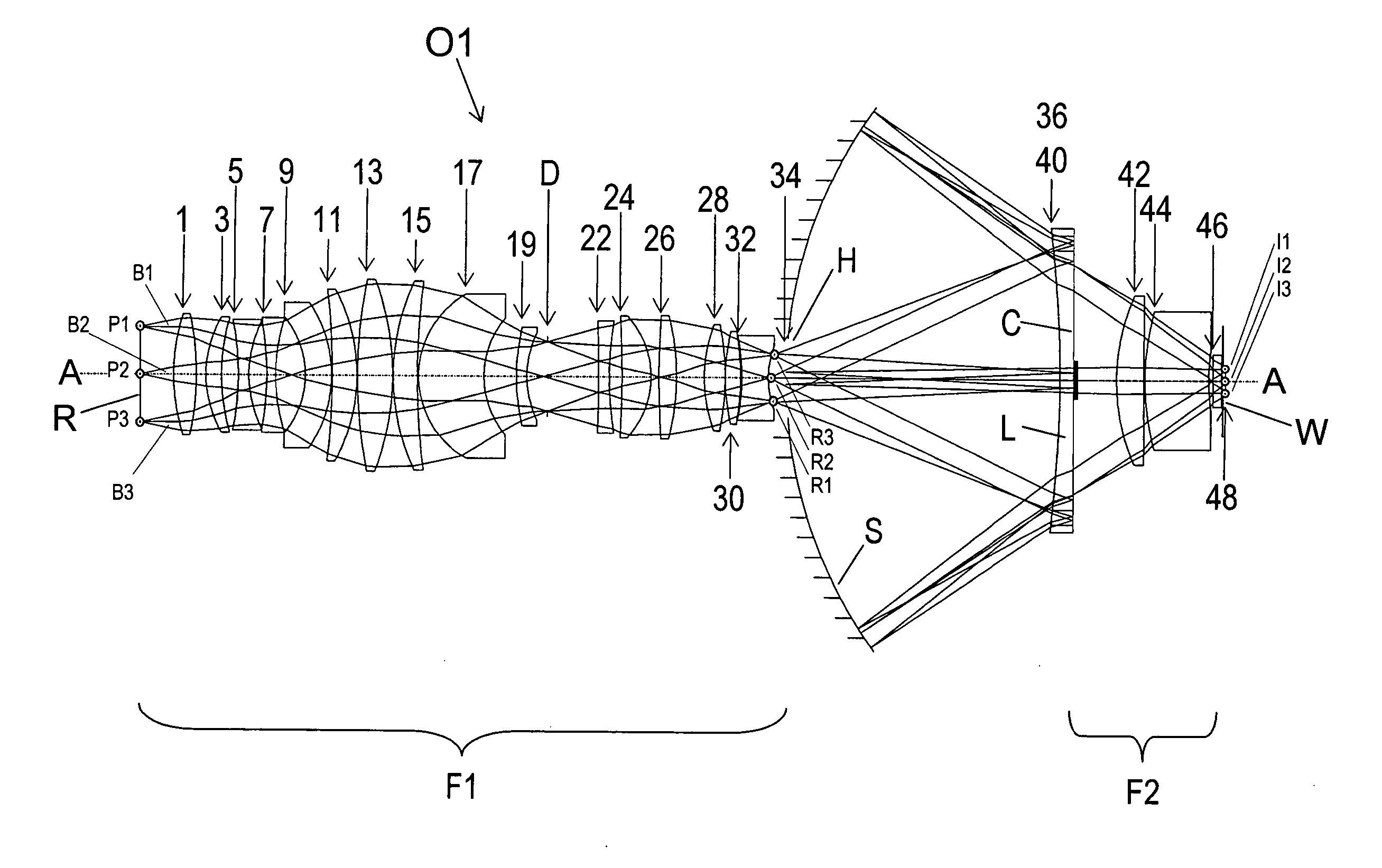
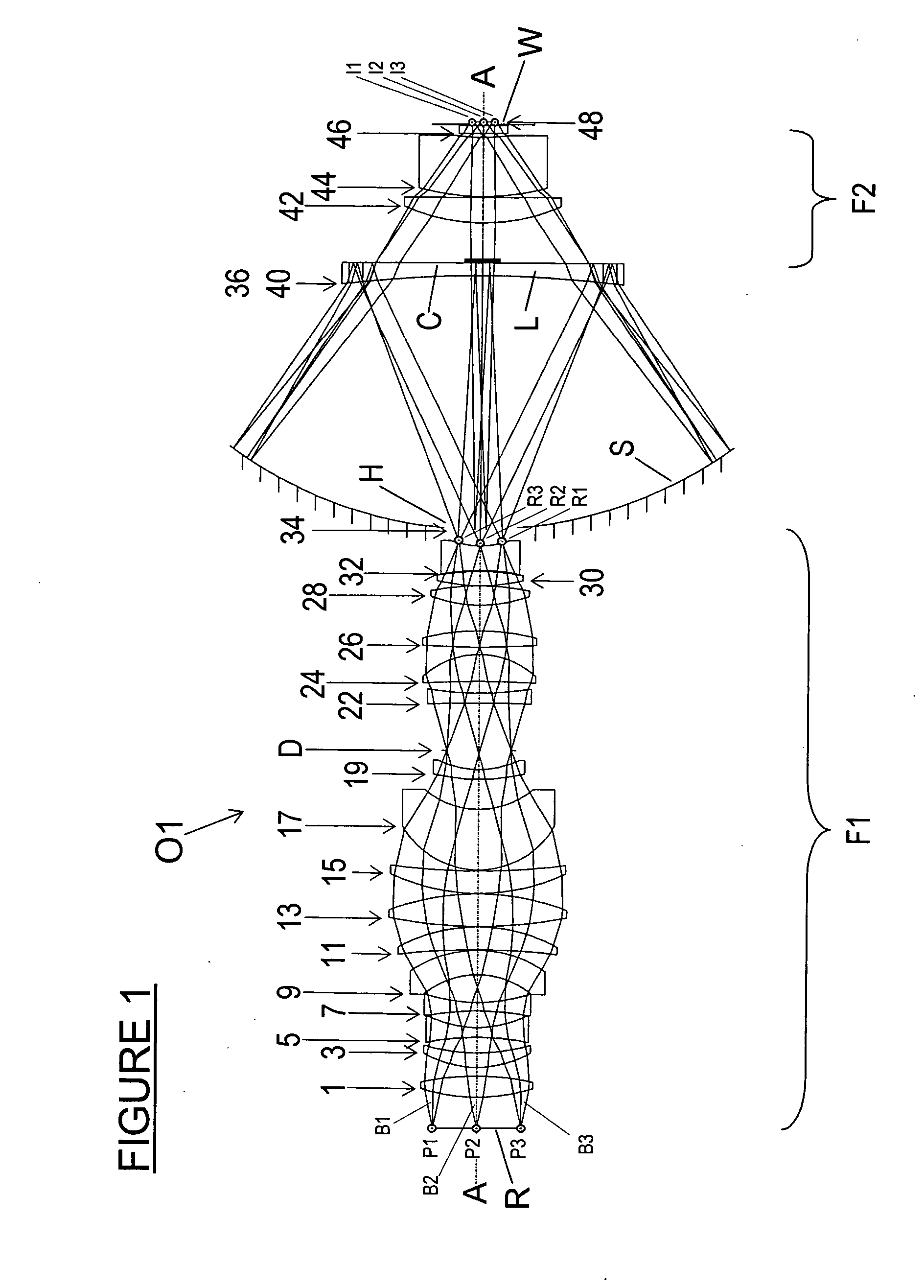
[0065]FIG. 1 illustrates a catadioptric projection objective O1 according to the invention. All elements of the objective, i.e., the lenses of the first optical subsystem F1, the concave mirror S, the lens L with the beam splitter coating, and the third optical subsystem F2 are aligned and centered on the optical axis represented by the line A-A in FIG. 1. A micro-structured mask R (also referred to as a reticle R) is arranged in the object plane, and a wafer W with a light-sensitive coating is arr...


PUM


Abstract

A catadioptric objective for a microlithography projection system has an in-line single-axis arrangement of lenses and reflectors. The catadioptric portion of the objective includes a catadioptric lens element with at least one reflective surface or surface portion reflecting light back into the lens, so that the catadioptric lens element interacts with light rays through reflection as well as refraction.

Description

BACKGROUND OF THE INVENTION [0001] The invention relates to a catadioptric projection objective for a microlithographic exposure apparatus used in producing microstructured devices such as integrated circuits or other semiconductor devices. Such devices are fabricated in a photolithography process in which a mask (also referred to as reticle) representing a microstructured circuit pattern is positioned in the object plane of a projection objective. A reduced copy of the pattern is produced photographically on a semiconductor wafer positioned in the image plane of the projection objective. [0002] In order to obtain the highest possible image resolution in the reproduction of the microscopically fine structures, it is desirable to increase the numerical aperture on the image side of the projection objective and to employ light of a shorter wavelength, preferably in the ultraviolet range of the spectrum with wavelengths that are typically shorter than about 260 nanometers. [0003] Howev...

Claims


Application Information

Patent Timeline
Patent Type & Authority Applications(United States)
IPC IPC(8): G02B17/00
CPCG02B17/08G02B17/0808G02B17/0856G02B17/0892G03F7/70225
Inventor SHAFER, DAVID R.EPPLE, ALEXANDERULRICH, WILHELM
Owner CARL ZEISS SMT GMBH
Learn More