Semiconductor light emitting device, backlight device for liquid crystal display

a technology of semiconductor lasers and light beams, which is applied in the direction of semiconductor lasers, semiconductor/solid-state device details, instruments, etc., can solve the problems of reducing the achieve the reduction of directional characteristics of light beams, similar optical directional characteristics, and improved luminance efficiency of light beams incident on optical waveguides

Active Publication Date: 2006-04-20
SHARP KK
View PDF8 Cites 54 Cited by
  • Summary
  • Abstract
  • Description
  • Claims
  • Application Information

AI Technical Summary

Benefits of technology

[0016] According to the arrangement, by aligning and spacing the first concave portions from each other with an equal pitch on a linear line, it is possible to equalize distances between light beams emitted from the light emitting elements and wall surfaces of the first concave portions, and distances between the light beams and wall surfaces of the second concave portions. Accordingly, the light beams emitted from the light emitting elements have a similar optical directional characteristic. This reduces variations in the directional characteristics of the light beams, which has been a problem in a conventional structure.
[0018] According to the arrangement, by aligning and spacing the first concave portions from each other with an equal pitch on a linear line parallel to the one edge portion of the package substrate, it is possible to equalize distances between light beams emitted from the light emitting elements and wall surfaces of the first concave portions, and distances between the light beams and wall surfaces of the package substrate. Accordingly, the light beams emitted from the light emitting elements have similar optical directional characteristics. This reduces variations in the directional characteristics of the light beams, which has been a problem in a conventional structure.
[0019] Thus, by installing the semiconductor light emitting device to an optical waveguide of a backlight device, luminance efficiency of the light beams incident on the optical waveguide can be improved. This is because the light beams have reduced gradients with respect to a light incident surface of the optical waveguide, thereby being projected on the optical waveguide at an approximately square angle from the light incident surface of the optical waveguide.
[0020] As a result, with the foregoing structure, the luminance efficiency of the light beams incident on the optical waveguide can be improved. This facilitates guiding more amount of light into the optical waveguide, and enhances the brightness of the light beams emitting from the optical waveguide. Thus, in a backlight device for an LCD, it is possible to set a high brightness of image display in the LCD, so that quality of the image display can be improved.

Problems solved by technology

This reduces variations in the directional characteristics of the light beams, which has been a problem in a conventional structure.

Method used


Image

  • Semiconductor light emitting device, backlight device for liquid crystal display
  • Semiconductor light emitting device, backlight device for liquid crystal display
  • Semiconductor light emitting device, backlight device for liquid crystal display

Examples


first embodiment

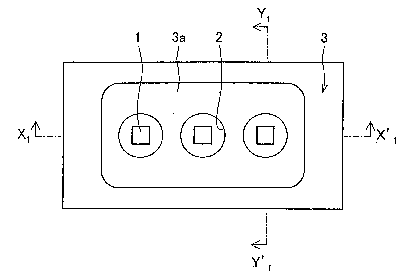
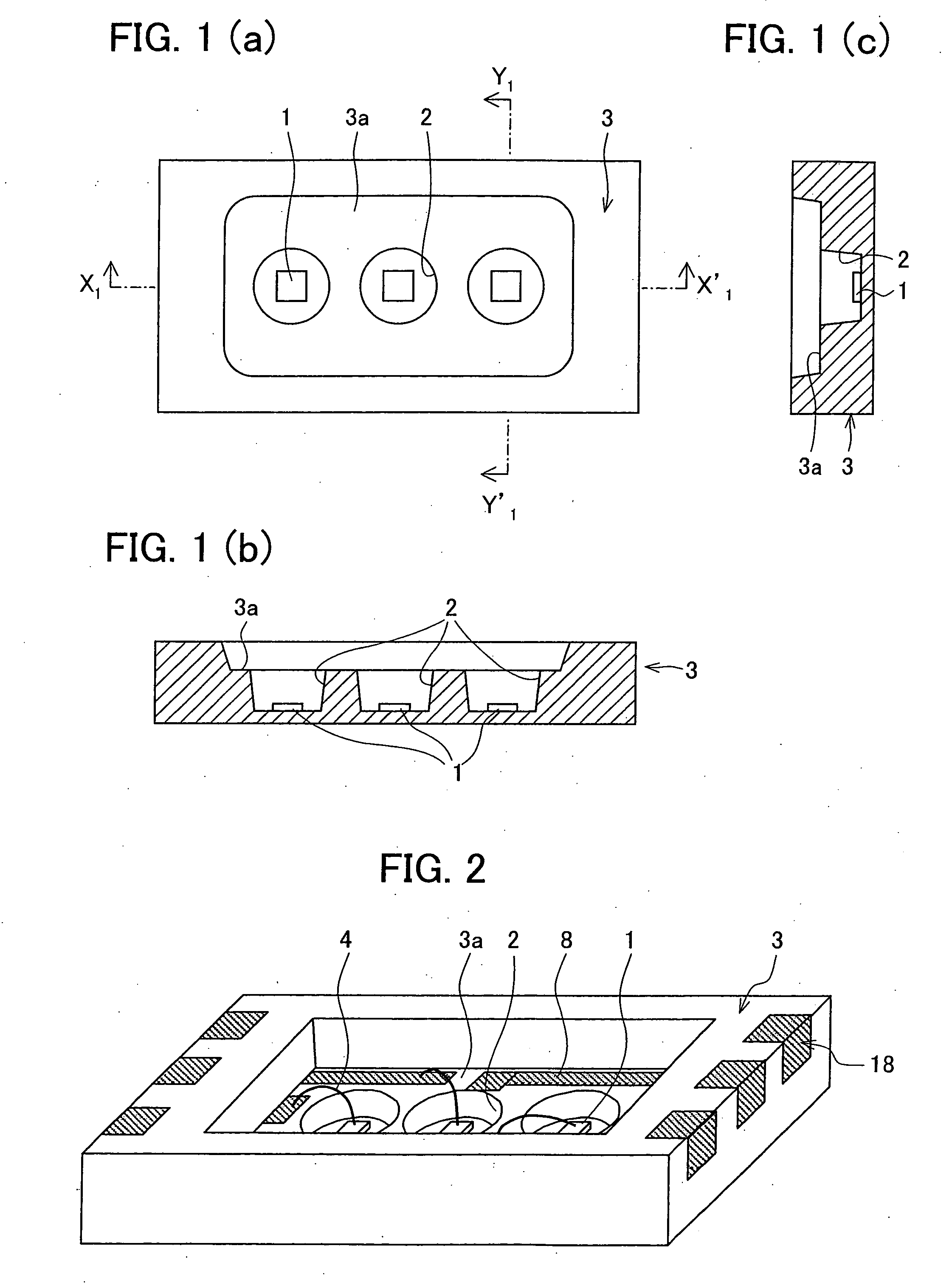
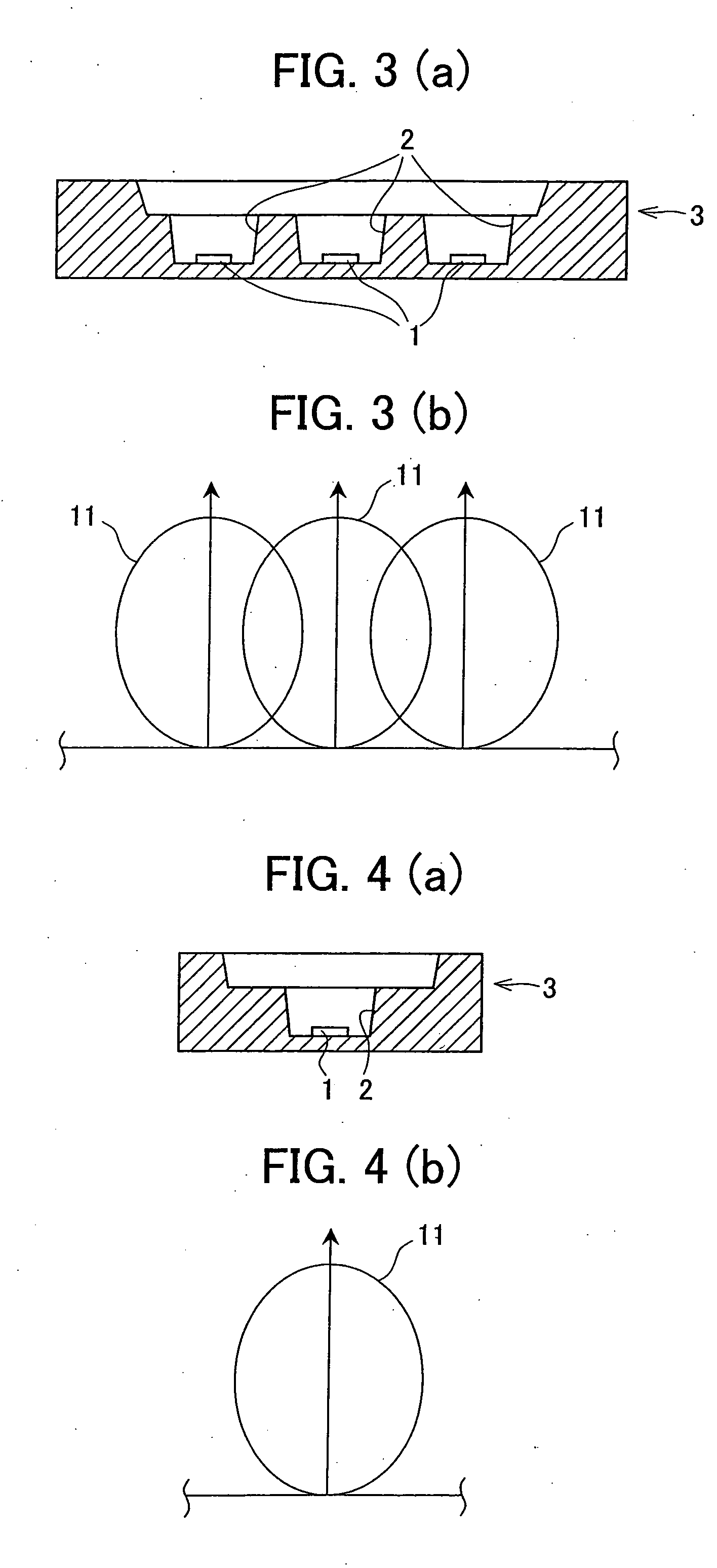
[0047] As illustrated in FIGS. 1 and 2, a semiconductor light emitting device (lighting device) according to one embodiment of the present invention has a plurality of (e.g. three) light emitting elements 1 in a package body 3 used in a semiconductor light emitting device, which is formed in a substantially rectangular plate. Examples of the light emitting element 1 are an LED and a semiconductor laser, which are formed in substantially rectangular solids. The package body 3 may be made of an electrical insulator having good heat conductance. Examples of materials of the package body 3 are: (i) a ceramics such as a silicon carbide (SiC), an alumina (AL2O3), or an aluminum nitride (AlN); (ii) a reinforcing resin such as an epoxy resin reinforced by glass fiber or carbon fiber; or (iii) a metal frame or a material made of a resin which holds the metal frame and reflects light. Regarding brightness and formability, an aluminum nitride is preferable.

[0048] The insulator refers to elect...

second embodiment

[0064] According to a second embodiment, as the sealing resin section 5, a fluorescent material mixed resin is used instead of the transparent resin described in the first embodiment. As illustrated in FIG. 6, blue color light emitting elements are used as the light emitting elements 1. Further, one of the mounting concave portions 2 is set to pass blue light from the blue color light emitting element. Another one of the mounting concave portions 2 is filled with a sealing resin section 5a in which a first fluorescent material is mixed. The first fluorescent material emits green light from blue light emitted from the blue color light emitting element. Further, a further one of the mounting concave portions 2 is filled with a sealing resin section 5b in which a second fluorescent material is mixed. The second fluorescent material emits red light from blue light emitted from the blue color light emitting element.

[0065] According to the second embodiment, each of the fluorescent mater...

third embodiment

[0068] According to a third embodiment, as the sealing resin section 5, a fluorescent material mixed resin is used instead of the transparent resin described in the first embodiment. As illustrated in FIG. 7, ultraviolet light emitting elements are used as the light emitting elements 1. One of the mounting concave portions 2 is filled with a sealing resin section 5c in which a fourth fluorescent material is mixed. The fourth fluorescent material emits blue light from ultraviolet light emitted from the ultraviolet light emitting element. Another one of the mounting concave portions 2 is filled with a sealing resin section 5d in which a fifth fluorescent material is mixed. The fifth fluorescent material emits green light from ultraviolet light emitted from the ultraviolet light emitting element. Further, a further one of the mounting concave portions 2 is filled with a sealing resin section 5e in which a sixth fluorescent material is mixed. The sixth fluorescent material emits red lig...


PUM


Abstract

A semiconductor light emitting device of the present invention includes a plurality of light emitting elements, a package body for storing the light emitting elements, wiring patterns being electrically connected to the light emitting elements, and Au wires for electrically connecting the light emitting elements and the wiring patterns, the package body including mounting concave portions for storing the respective light emitting elements, and storing concave portion for storing the mounting concave portions and the Au wires, the mounting concave portions being aligned on a linear line and spaced from each other with an equal pitch. In the above arrangement, as the semiconductor light emitting device of the present invention, it is possible to provide a semiconductor light emitting device having a high directional characteristic of emitted light, and a backlight device for a liquid crystal display, the backlight device using the semiconductor light emitting device and having an improved brightness of the emitted light.

Description

[0001] This Nonprovisional application claims priority under 35 U.S.C. § 119(a) on Patent Application No. 2004 / 303503 filed in Japan on Oct. 18, 2004, the entire contents of which are hereby incorporated by reference. FIELD OF THE INVENTION [0002] The present invention relates to a semiconductor light emitting device as a preferable light source for a liquid crystal display (hereinafter referred as LCD), and a backlight device for an LCD, the backlight device using the semiconductor light emitting device. BACKGROUND OF THE INVENTION [0003] Conventionally, a cold cathode tube has been used as a light source for a backlight in a display such as an LCD. The cold cathode tube requires a high frequency and high voltage of up to about 2000 Vrms when lighting. Therefore, in a display using the cold cathode tube, safety on insulation for the generated high frequency and high voltage has to be ensured, which requires special attention to careful packaging, insulation, prevention of noise, or...

Claims


Application Information

Patent Timeline
Patent Type & Authority Applications(United States)
IPC IPC(8): H01S5/00H01L33/50H01L33/62
CPCG02F1/133603H01L25/0753H01L33/60H01L33/62H01S5/005H01S5/02216H01S5/02228H01S5/02284H01S5/4025H01L2224/48091H01L2924/00014H01S5/02276H01L2924/00H01L2924/01322H01L2224/45144H01L2224/45124H01L2924/3025H01S5/02234H01S5/02251H01S5/02345
Inventor INOGUCHI, TSUKASA
Owner SHARP KK
Why Eureka
Try Eureka