Semiconductor device and manufacturing method thereof

a technology of semiconductors and semiconductors, applied in the direction of semiconductor devices, electrical devices, transistors, etc., can solve the problems of increasing the number of steps and the complexity of the manufacturing process of transistors, and achieve the effect of improving the efficiency of the manufacturing process and reducing the number of steps

Inactive Publication Date: 2006-05-04
RENESAS TECH CORP
View PDF7 Cites 15 Cited by
  • Summary
  • Abstract
  • Description
  • Claims
  • Application Information

AI Technical Summary

Benefits of technology

[0017] A manufacturing method of a n channel MIS transistor and a p channel MIS transistor according to the present invention comprises the steps of: (a) forming a gate insulator mainly containing metal oxide on a main surface of a semiconductor substrate; (b) after forming a metal film mainly containing noble metal with catalytic reduction effect on the gate insulator, patterning the metal film, thereby forming a gate electrode of the n channel MIS transistor on the gate insulator in the first region and forming a gate electrode of th

Problems solved by technology

However, in the conventional technology in which the gate electrode of the n channel MIS transistor and the gate electrode of the p channel MIS transist

Method used


Image

  • Semiconductor device and manufacturing method thereof
  • Semiconductor device and manufacturing method thereof
  • Semiconductor device and manufacturing method thereof

Examples


first embodiment

(First Embodiment)

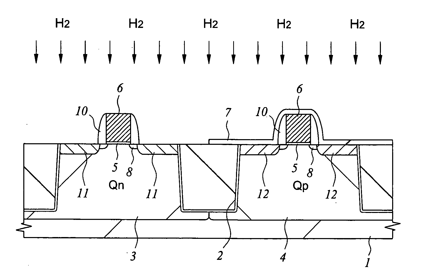
[0041] The manufacturing method of a n channel MIS transistor and a p channel MIS transistor according to the first embodiment will be described with reference to FIG. 1 to FIG. 12.

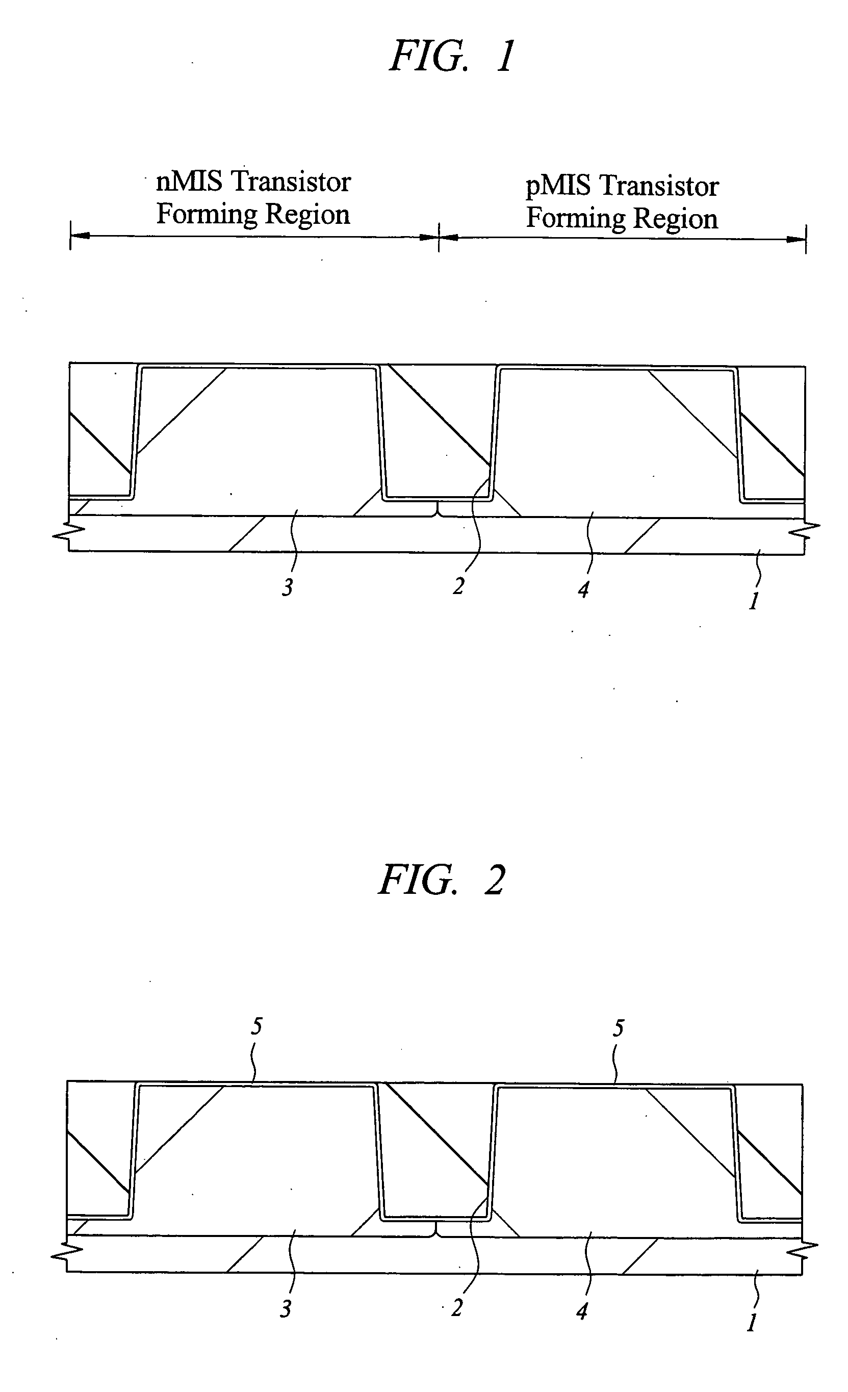
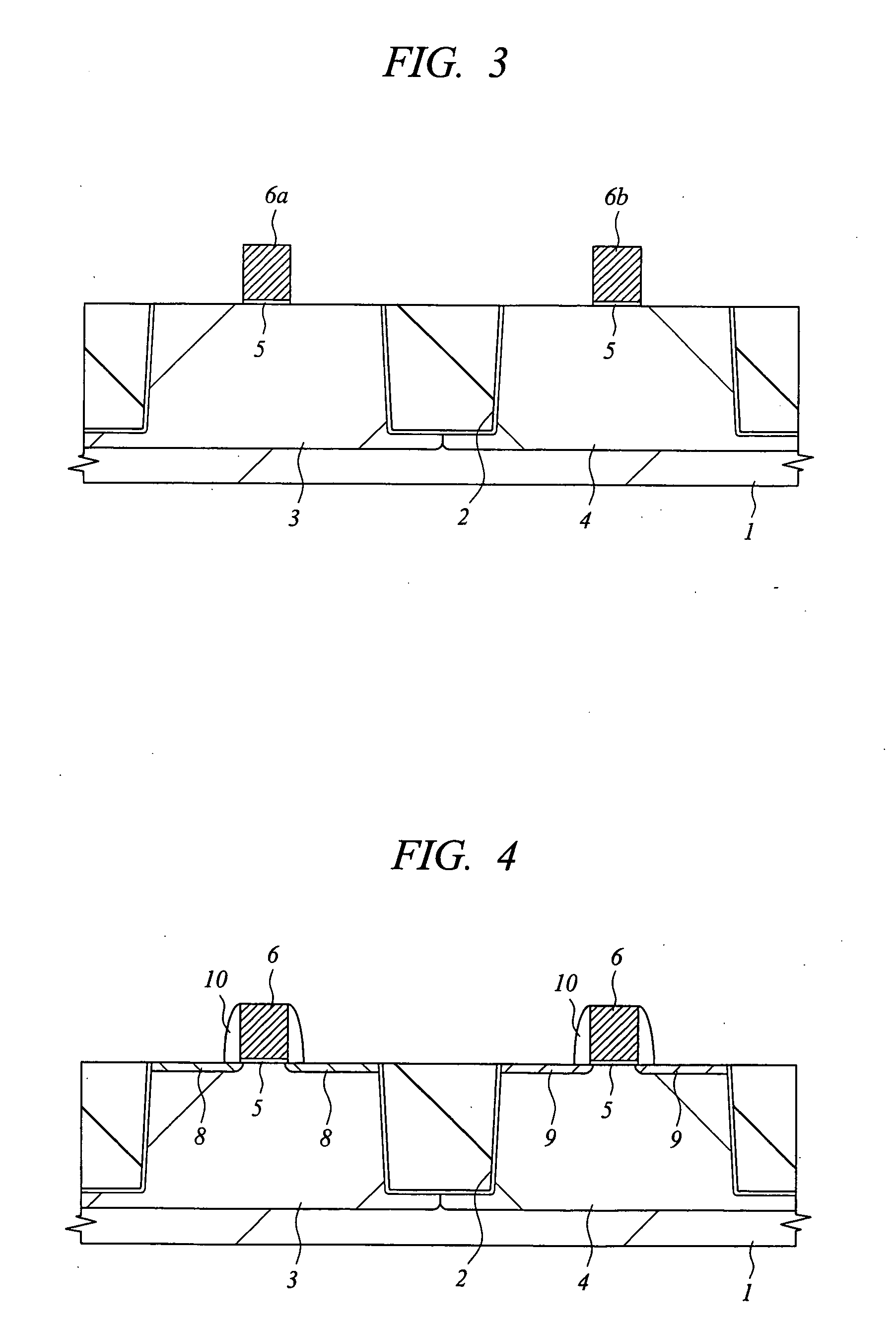
[0042] First, as shown in FIG. 1, a device isolation trench 2 is formed in the main surface of the semiconductor substrate (hereinafter, referred to as substrate) 1 made of p type single crystal silicon by using the well-known STI (Shallow Trench Isolation) technology. Thereafter, boron is ion-implanted into a n channel MIS transistor forming region (left side of FIG. 1) of the substrate 1, and phosphorus is ion-implanted into a p channel MIS transistor forming region (right side of FIG. 2) of the substrate 1. Subsequently, the impurities (boron and phosphorus) are diffused in the substrate 1 by the thermal treatment of the substrate 1, thereby forming a p type well 3 and a n type well 4 in the main surface of the substrate 1.

[0043] Next, impurities for adjusting the threshold voltage ...

second embodiment

(Second Embodiment)

[0060] The manufacturing method of a n channel MIS transistor (Qn) and a p channel MIS transistor (Qp) according to the second embodiment will be described with reference to FIG. 13 to FIG. 21.

[0061] First, by the same method as described in the first embodiment with reference to FIG. 1, the device isolation trenches 2, the p type well 3 and the n type well 4 are formed in the main surface of the substrate 1. Subsequently, impurities for adjusting the threshold voltage of the MIS transistors are ion-implanted into the surfaces of the p type well 3 and the n type well 4. Next, as shown in FIG. 13, a silicon oxide film 20 is formed on each of the surfaces of the p type well 3 and the n type well 4 by the thermal treatment of the substrate 1.

[0062] Next, as shown in FIG. 14, after depositing a polycrystalline silicon film (or amorphous silicon film) on the substrate 1 by the CVD, the polycrystalline silicon film is patterned by the dry etching using a photoresist f...


PUM


Abstract

The manufacturing process of a semiconductor device in which a n channel MIS transistor and a p channel MIS transistor each having a gate electrode made of a metal material formed on a gate insulator made of a high dielectric constant material are used to form a CMOS circuit is simplified. After simultaneously forming the gate electrodes of the n channel MIS transistor and the p channel MIS transistor by patterning a platinum film deposited on a gate insulator made of a hafnium oxide film, only the gate insulator on the side of the n channel MIS transistor is selectively reduced by using the catalytic reduction of the platinum film. By doing so, the work function of the gate electrode of the n channel MIS transistor is changed.

Description

CROSS-REFERENCE TO RELATED APPLICATION [0001] The present application claims priority from Japanese Patent Application No. JP 2004-314896 filed on Oct. 29, 2004, the content of which is hereby incorporated by reference into this application. TECHNICAL FIELD OF THE INVENTION [0002] The present invention relates to a semiconductor device and a manufacturing method thereof. More particularly, it relates to a technology effectively applied to a semiconductor device in which a n channel MIS transistor and a p channel MIS transistor each having a metal gate electrode formed on a gate insulator made of a high dielectric constant material such as hafnium oxide are used to form a CMOS (Complementary Metal Oxide Semiconductor) circuit. BACKGROUND OF THE INVENTION [0003] Conventionally, in the n channel MOS transistor and the p channel MOS transistor which constitute a CMOS circuit, a silicon oxide film is used as a gate insulator material, and a polycrystalline silicon film or a laminated fil...

Claims


Application Information

Patent Timeline
IPC IPC(8): H01L29/76
CPCH01L21/823842
Inventor NABATAME, TOSHIHIDEKADOSHIMA, MASARU
Owner RENESAS TECH CORP
Why Eureka
Try Eureka