Deployment of electro-optic amplitude varying elements (AVEs) and electro-optic multi-functional elements (MFEs) in photonic integrated circuits (PICs)

a technology multi-functional elements, which is applied in the field of photonic integrated circuits, can solve the problems of limiting the overall reach of the optical transmission system, the performance of the optical transmission network or optical transport system, and the optical signal-to-noise ratio (osnr), so as to improve the optical isolation of the laser source, avoid possible waveform degradation, and improve wavelength stability

Inactive Publication Date: 2006-05-04
INFINERA CORP
View PDF35 Cites 53 Cited by
  • Summary
  • Abstract
  • Description
  • Claims
  • Application Information

AI Technical Summary

Benefits of technology

[0013] It is an object of this invention to enhance the dynamic range of an optical communication system by deployment of per channel integrated amplitude varying elements (AVEs) and / or multi-functional elements (MFEs) in a photonic integrated circuit (PIC), including but not limited to, a transmitter photonic integrated circuit (TxPIC) or in a receiver photonic integrated circuit (RxPIC).
[0031] On the other hand, SOAs, rather than VOAs or photodetectors functioning as a VOA, may be employed for power equalization across the channel array. In this case, however, back reflections in the signal channels may be amplified rather than attenuated, as in the case of VOAs or FPDs, so that it may be preferred to include an integrated, optical waveguide isolator in each channel to protect the channel laser source from back reflections that may cause the laser source from becoming unstable, in particular, change its emission wavelength or its optical spectrum. Such optical waveguide isolators are known in the art particularly as discrete active or passive elements and find uses in optical communication systems. The purpose of an optical isolator is to eliminate unwanted or reflected optical signals from interfering with a desired optical function. For example, an optical waveguide isolator may be inserted in an optical signal path between a distributed feedback (DFB) laser and an optical fiber. Without the isolator, unwanted optical signals (i.e., reflections) from the optical fiber would couple back into the DEB laser and adversely affect its transmitted optical spectrum. By including an isolator in such situations, unwanted reflected signals are absorbed by the isolator and do not reach the laser source. Such optical isolators have not been proposed or used in conjunction with TxPICs.

Problems solved by technology

An optical transmission network or an optical transport system is limited in performance due to several issues.
The primary issues are optical signal-to-noise ratio (OSNR) at both the optical transmitter and receiver, the Q at both the optical transmitter and receiver, and the dynamic range of the optical receiver, i.e., the level of ability to receive distorted channel optical signals and still interpret the data represented by the information modulated on the channel signals sent from the optical transmitter.
The accumulative effect of the foregoing is to limit the overall reach of the optical transmission system or, alternatively, to increase the cost of the system.
Even if the transmitted channel signals are equalized, they arrive at the receiver distorted with variations among the optical signal levels resulting in an unacceptable level of transmission errors.
AVEs such as SOAs, VOAs, ZOAs (combination SOA / VOAs) or monitoring photodetectors (PDs) functioning also as a reverse bias AVEs or like VOAs when placed in different locations in PIC signal channel paths can have detrimental affects on the channel modulated signal.
However, the added channel AVEs may have some affect one the optical modulated signal shape and the signal optical spectrum so that it becomes important as to where such AVEs may be placed in the signal channel paths to achieve optimum performance in terms of modulated signal output substantially unaffected by AVE operation.

Method used


Image

  • Deployment of electro-optic amplitude varying elements (AVEs) and electro-optic multi-functional elements (MFEs) in photonic integrated circuits (PICs)
  • Deployment of electro-optic amplitude varying elements (AVEs) and electro-optic multi-functional elements (MFEs) in photonic integrated circuits (PICs)
  • Deployment of electro-optic amplitude varying elements (AVEs) and electro-optic multi-functional elements (MFEs) in photonic integrated circuits (PICs)

Examples


second embodiment

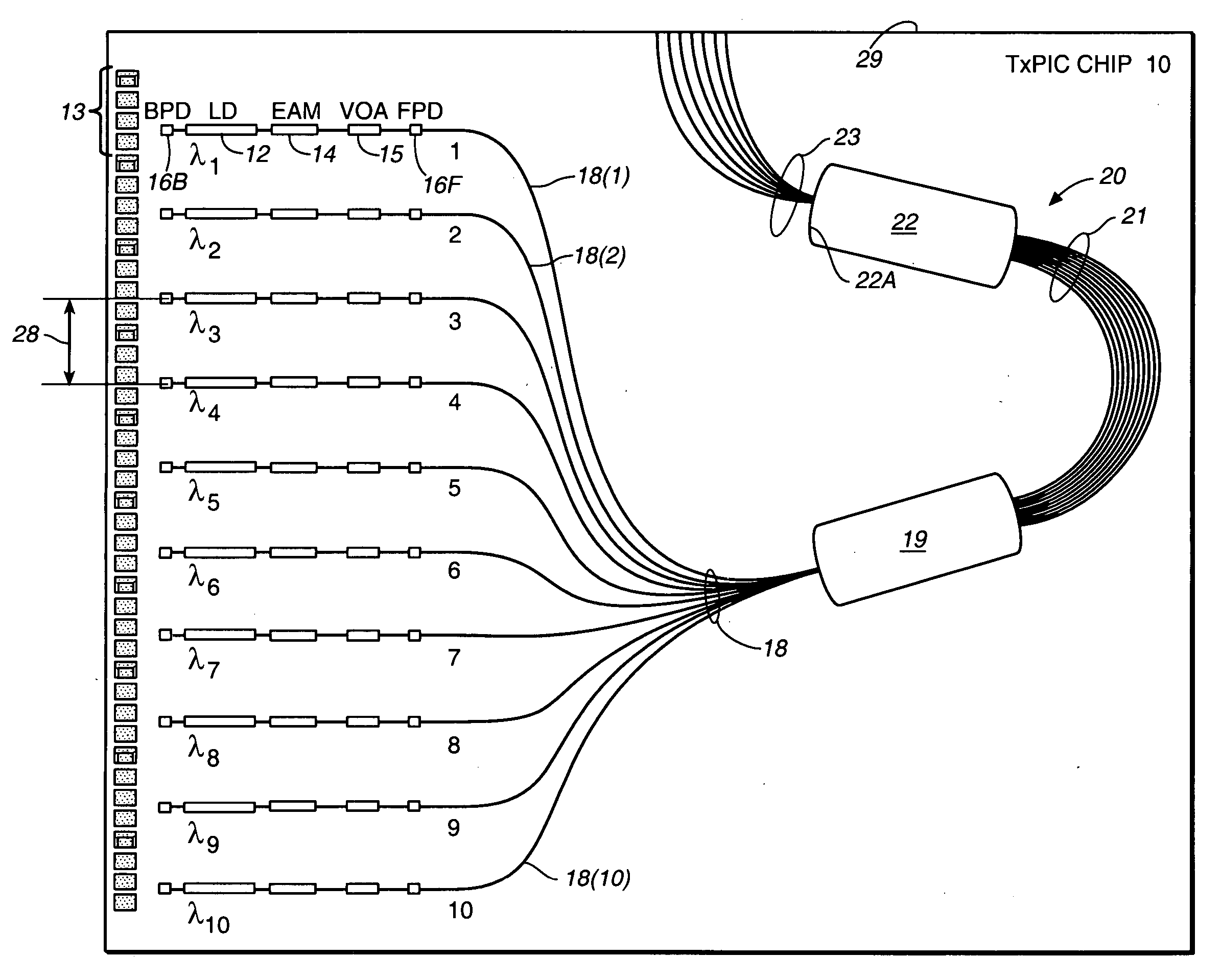
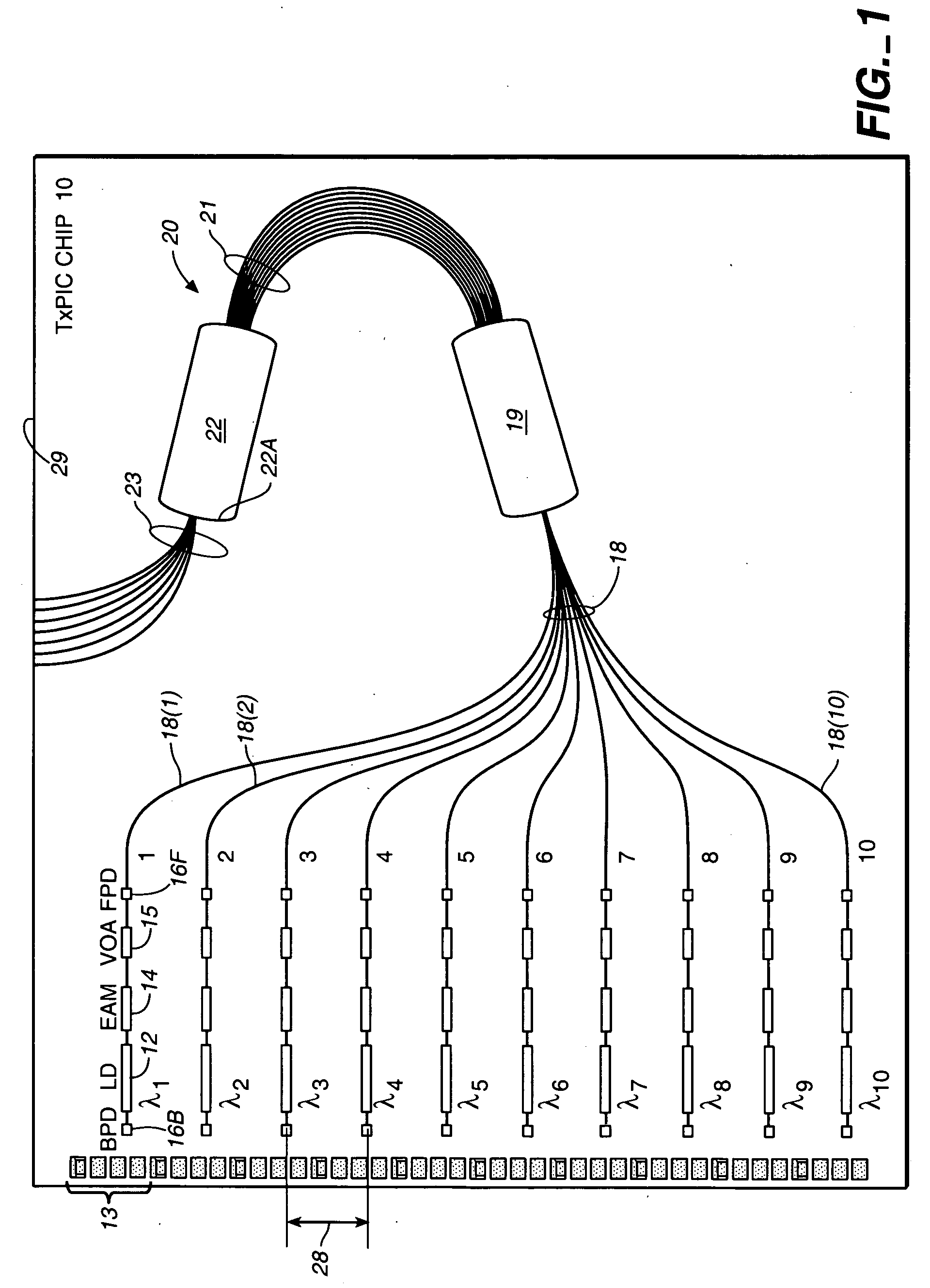
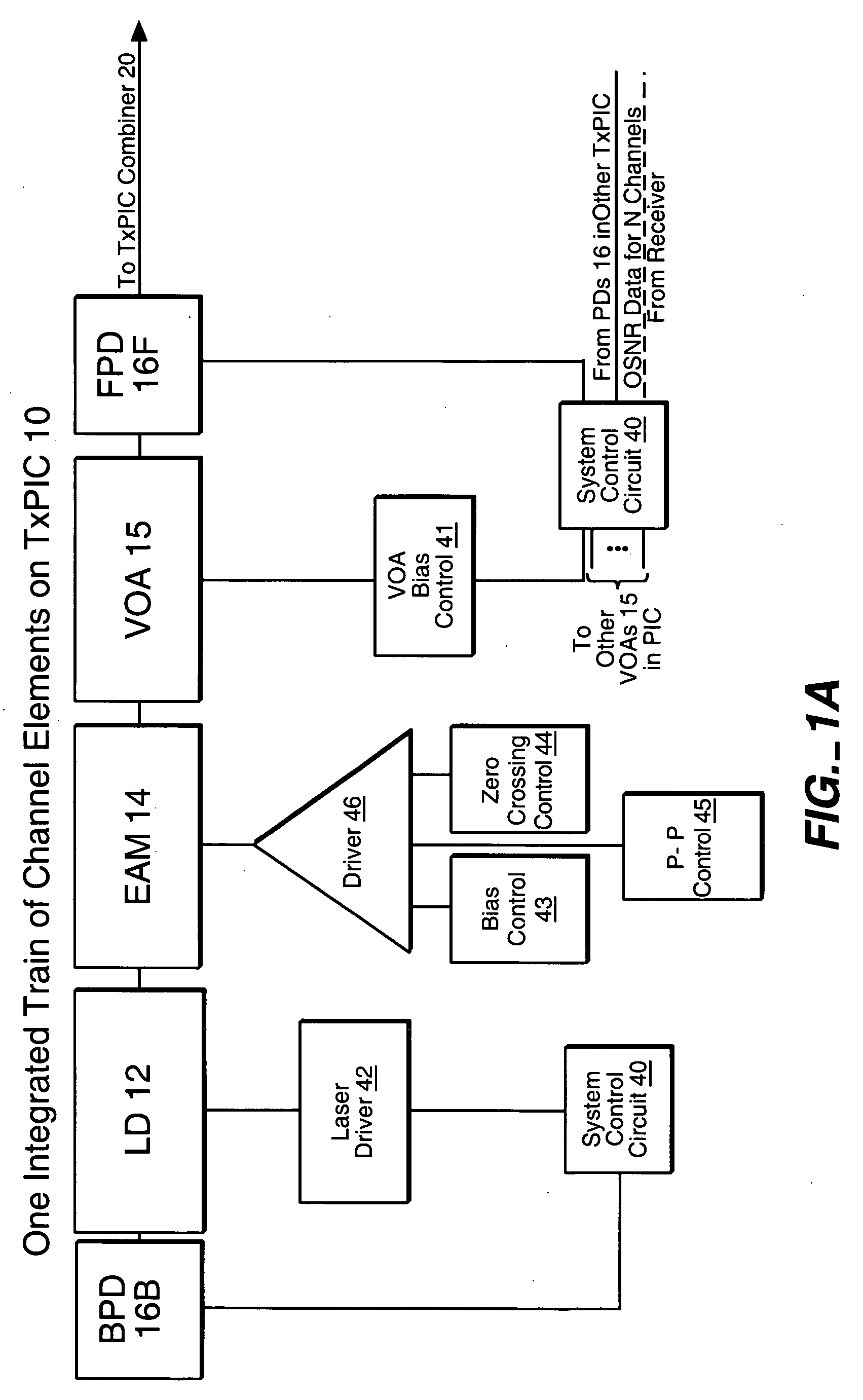
[0062] Reference is now made to the second embodiment shown in FIG. 2 comprising TxPIC chip 10A which is identical to FIG. 1 except the electro-optic amplitude varying element (AVE) shown here in the form of variable optical attenuator 15 is illustrated as positioned in each signal channel between laser source 12 and electro-optic modulator 14. A primary reason for placing VOA 15 before modulator 14 is that, placed in the position as illustrated in FIG. 1, VOA 15 may possibly degrade the Q quality or provide a Q penalty to the modulated signal output from modulator 14 including possibly some phase change to the signal. More will be said about this in connection with the embodiment shown in FIG. 10. Again, the system control circuit 40 may be employed in FIG. 2 as well as in other described embodiments to provide for pre-emphasis in the manner described in connection with that figure.

first embodiment

[0063] Reference is now made to a third embodiment of this invention in FIG. 3 comprising TxPIC chip 10B which is the same as the first embodiment in FIG. 1 except that the electro-optic amplitude varying element (AVE) illustrated here is a semiconductor optical amplifier (SOA) 19 placed in each signal channel 1 to 10 after modulator 14. The function of SOA 19 is to provide equalization across the array of λ1-λN channels by amplifying those modulated signals that are below a desired power level or to apply gain to N−1 channel signals as necessary to increase the signal gain to that of the naturally highest gain signal channel. It should be noted that with an SOA 19 or a VOA 15 provided after modulator 14, these amplitude varying elements (AVEs) may add an additional chirp to the channel modulated signal which may, in some cases, be used advantageously to predistort the signal to achieve some dispersion compensation toward improving the BER at the optical receiver across the optical ...

third embodiment

[0064] Reference is now made to a fourth embodiment of this invention shown in FIG. 4 comprising TxPIC chip 10C which is the same as the third embodiment in FIG. 3 except that semiconductor optical amplifier (SOA) 19 placed in each signal channel before modulator 14. Care must be taken in the implementation of this embodiment that SOA 19 is not sufficiently biased as to place modulator 14 into saturation. More is said about this embodiment later on in connection with the embodiment of FIG. 11.


PUM


Abstract

Electro-optic amplitude varying elements (AVEs) or electro-optic multi-function elements (MFEs) are integrated into signal channels of photonic integrated circuits (PICs) or at the output of such PICs to provide for various optical controlling and monitoring functions. In one case, such PIC signal channels may minimally include a laser source and a modulator (TxPIC) and in another case, may minimally include a photodetector to which channels, in either case, an AVE or an MFE may be added.

Description

CROSS-REFERENCE TO RELATED APPLICATIONS [0001] This application is a continuation-in-part of subject matter disclosed in and claims priority to U.S. patent application Ser. No. 10 / 267,331, filed Oct. 8, 2002 and entitled, TRANSMITTER PHOTONIC INTEGRATED CIRCUITS (TxPIC) AND OPTICAL TRANSPORT NETWORKS EMPLOYING TxPICs, also published on May 22, 2003 as Pub. No. US2003 / 0095737 A1; U.S. patent application Ser. No. 10 / 267,330, filed Oct. 8, 2002 and entitled, TRANSMITTER PHOTONIC INTEGRATED CIRCUIT (TxPIC) CHIP ARCHITECTURES AND DRIVING SYSTEMS AND WAVELENGTH STABILIZATION FOR TxPICs, also published on May 22, 2003 as Pub. No. US2003 / 0095736 A1; and U.S. patent application Ser. No. 10 / 267,304, filed Oct. 8, 2002 and entitled, AN OPTICAL SIGNAL RECEIVER PHOTONIC INTEGRATED CIRCUIT (RxPIC), AN ASSOCIATED OPTICAL SIGNAL TRANSMITTER PHOTONIC INTEGRATED CIRCUIT (TxPIC) AND AN OPTICAL TRANSPORT NETWORK UTILIZING THESE CIRCUITS, also published on Feb. 19, 2004 as Pub. No. US2004 / 0033004 A1, an...

Claims


Application Information

Patent Timeline
Patent Type & Authority Applications(United States)
IPC IPC(8): H04J14/02
CPCG02B6/12004G02B6/12019G02B6/12026G02B6/4249G02B6/43H01S5/02248H01S5/0268H04J14/02H01S5/02325
Inventor WELCH, DAVID F.KISH, FRED A. JR.NAGARAJAN, RADHAKRISHNAN L.NILSSON, ALAN C.TAYLOR, ROBERT R.
Owner INFINERA CORP
Why Eureka
Try Eureka