Electrical system, especially a microelectronic or microelectromechanical high frequency system

a microelectronic or microelectromechanical high frequency system technology, applied in the direction of electrical equipment, semiconductor devices, semiconductor/solid-state device details, etc., can solve the problems of reducing the high-frequency properties of electrical components, requiring a large amount of space, and ensuring the requisite gas tightness or moistur

Inactive Publication Date: 2006-05-11
ROBERT BOSCH GMBH
View PDF13 Cites 7 Cited by
  • Summary
  • Abstract
  • Description
  • Claims
  • Application Information

AI Technical Summary

Benefits of technology

[0014] The electrical component according to the present invention and the method according to the present invention for manufacturing it have the advantage, as compared with the existing art, that the feedthroughs can be manufactured to be very much smaller than in the existing art; and that additional special adaptation structures for integration of those feedthroughs into a circuit having conductive structures for high-frequency electromagnetic waves, in particular in the range from 1 GHz to 80 GHz, can usually be dispensed with.
[0021] Lastly, a central problem in terms of protecting packaged or encapsulated high-frequency components or micromechanical components or sensor elements from external influences or the irradiation of electromagnetic fields is that of leading conductive structures that are connected to the packaged electrical high-frequency component out from an interior space enclosed by a capsule, since such leadthroughs must be configured to be on the one hand hermetically sealed and on the other hand compatible with high frequencies. An electrical component encapsulated according to a refinement of the invention advantageously avoids the problem of leading the conductive structures through the capsule by way of a backside contact through the base element, so that there is available around the encapsulated component an open area that can be used as a bonding surface for the capsule.

Problems solved by technology

The first problem that arises in this context is that of ensuring the requisite gas-tightness or moisture-tightness.
The feedthroughs for high-frequency microelectronic or microelectromechanical components known from the aforesaid publications have the disadvantage that they require a great deal of space because of the anisotropic wet etching of silicon using the (111) plane as the etching stop, and that the coplanar waveguides for high-frequency electromagnetic waves in the gigahertz region guided on the silicon substrates described therein must be provided with special electrical adaptation structures to allow them to be integrated into a corresponding high-frequency component.
These adaptation structures additionally result in a degradation of the high-frequency properties of the electrical components due to undesirable losses, a decrease in bandwidth, and the need for special impedance adaptation.

Method used


Image

  • Electrical system, especially a microelectronic or microelectromechanical high frequency system
  • Electrical system, especially a microelectronic or microelectromechanical high frequency system
  • Electrical system, especially a microelectronic or microelectromechanical high frequency system

Examples


Embodiment Construction

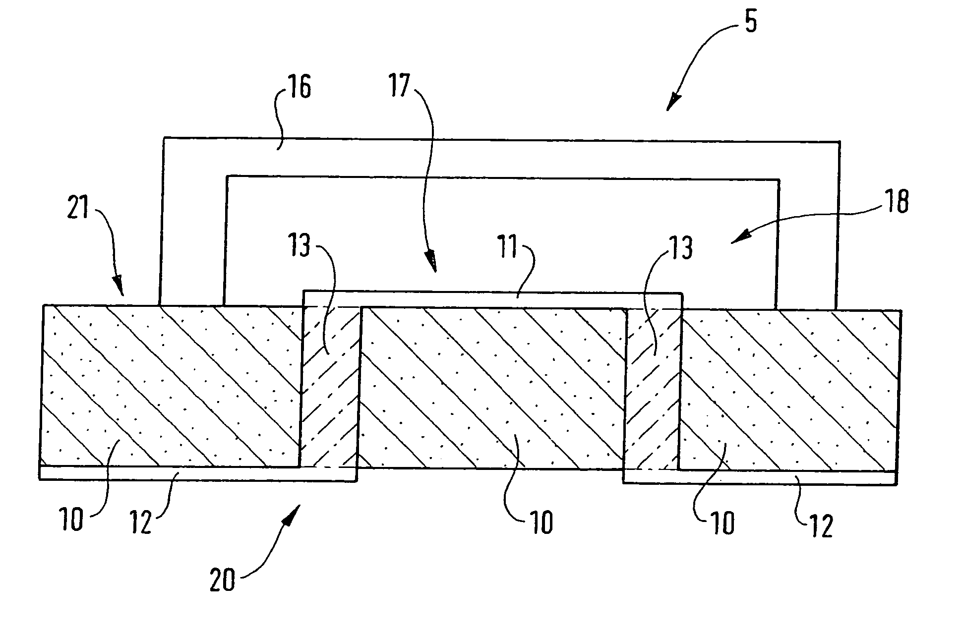
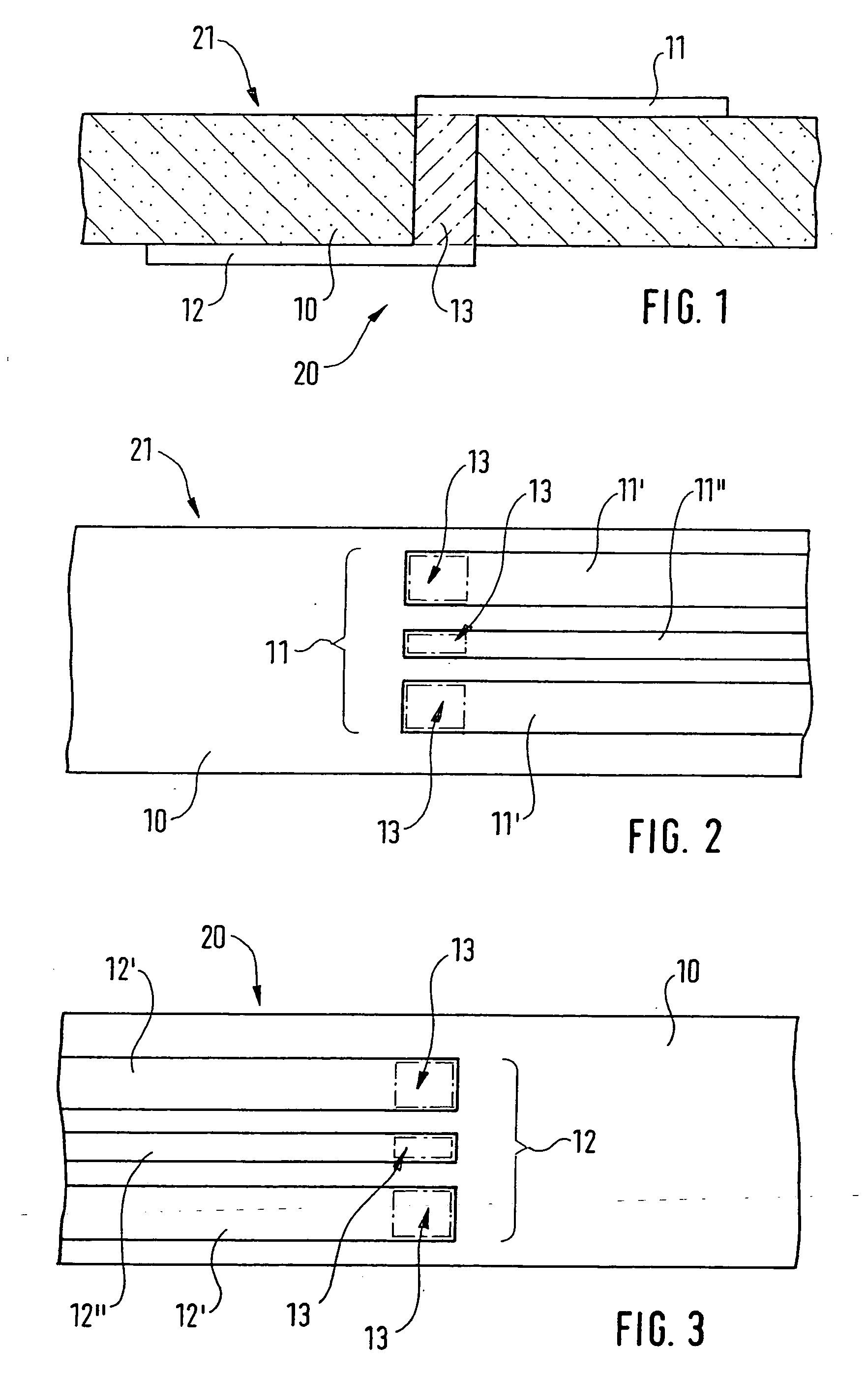
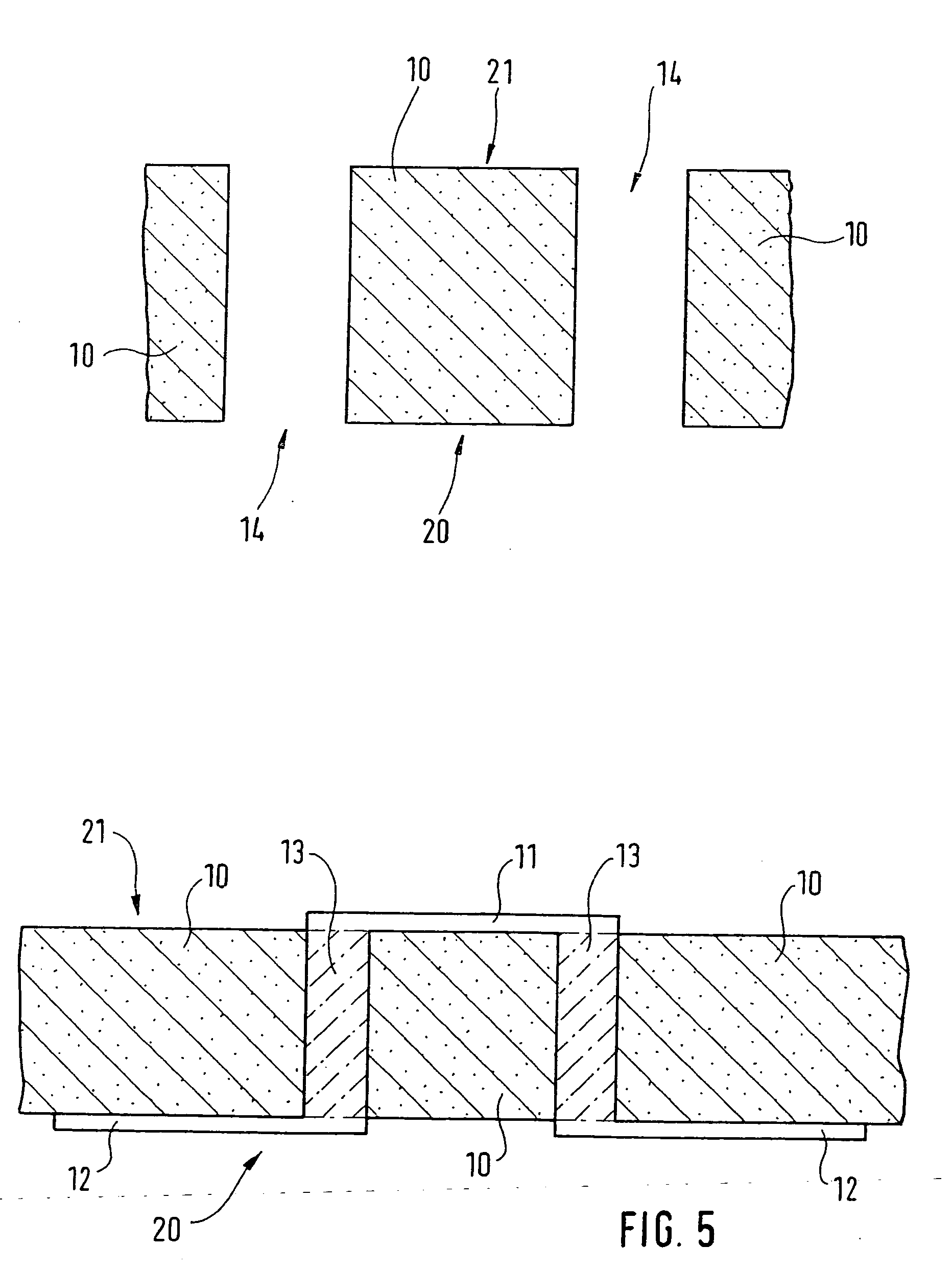
[0039]FIG. 1 explains a first exemplary embodiment for an electrical component 5 in the form of a high-frequency microelectronic component, a base element 10 in the form of a high-resistance silicon wafer having a specific electrical resistance of preferably more than 1000 Ω / cm being provided with a plurality of adjacent feedthroughs 13 or so-called “vias” that pass through base element 10 from its upper side 21 to its lower side 20. An upper conductive structure 11 is also provided on upper side 21, while a lower conductive structure 12 is located on lower side 20. Feedthroughs 13 are lined with a metal, for example gold, or another metal that can be deposited by electroplating. Lastly, provision is made for the lined feedthrough 13 to be connected in electrically conductive fashion to upper conductive structure 11 and to lower conductive structure 12, so that upper conductive structure 11 and lower conductive structure 12 are connected to one another continuously at least for high...


PUM


Abstract

An electrical component is proposed, in particular a high-frequency microelectronic or microelectromechanical component having a base element that is provided with a feedthrough, a first conductive structure extending on an upper side of the base element being connected by the feedthrough, continuously for high-frequency electromagnetic waves, to a second conductive structure extending on a lower side of the base element. The feedthrough has the form of a right prism or cylinder, and the first and / or the second conductive structure is embodied as a planar waveguide, in particular as a coplanar waveguide. Also proposed is a method for producing an electrical component having a feedthrough for high-frequency electromagnetic waves through a base element, an electrically conductive layer being applied on an upper side of the base element and an etching mask being applied on a lower side of the base element; a trench, having at least almost perpendicular sidewalls and penetrating through the base element, then being etched into the base element in a plasma etching step; an electrically conductive layer being applied on the lower side after the etching and after removal of the etching mask; and the trench lastly being filled or lined with an electrically conductive material.

Description

FIELD OF THE INVENTION [0001] The present invention relates to an electrical component, in particular a high-frequency microelectronic or microelectromechanical component, as well as a method for manufacturing the same. BACKGROUND INFORMATION [0002] German Published Patent Application No. 100 37 385 discloses a micromechanically fabricated high-frequency short-circuit switch that has a thin metal bridge which is extended between two ground leads of a coplanar waveguide. This high-frequency short-circuit switch is usable, for example, for adaptive cruise control (ACC) or short-range radar (SRR) applications in motor vehicles, and is operated at operating frequencies of typically 24 or 77 gigahertz. [0003] Many other microstructured or microsystem-engineering components are known besides, for example for applications in silicon-based high-frequency technology. These are also referred to as MEMS (microelectromechanical structures or systems) or HF-MEMS (high-frequency microelectromecha...

Claims


Application Information

Patent Timeline
Patent Type & Authority Applications(United States)
IPC IPC(8): H01L23/34H01L23/66H01P1/04H01P11/00
CPCH01L23/66H01L2223/6616H01L2223/6627H01L2924/15313H01L2924/16152H01L2924/1903H01L2924/3011H01P1/047H01P11/00
Inventor BREITSCHWERDT, KLAUSULM, MARKUSURBAN, ANDREAREIMANN, MATHIAS
Owner ROBERT BOSCH GMBH
Why Eureka
Try Eureka