Tiled construction of layered materials

Inactive Publication Date: 2006-05-18
SALMON TECH
View PDF6 Cites 16 Cited by
  • Summary
  • Abstract
  • Description
  • Claims
  • Application Information

AI Technical Summary

Benefits of technology

[0008] In a preferred embodiment, first material PI 2731 is chosen for its close CTE match with copper. PI 2731 will adhere well to the preferred copper substrate, even as the temperature is raised and lowered during temperature cycles. For each tiled dielectric layer on the copper substrate, PI 2731 is formed into intersecting grid lines that adhere well to the substrate or to layers previously fabricated on the substrate. Since the build-up layers are typically thin compared with the substrate, expansion behavior is normally dominated by the copper substrate element, with additional urging by the embedded copper conductors. Cytop is chosen as the second material for its excellent dielectric properties, and is deposited so as to form islands bounded by the grid lines of PI 2731. This tiled dielectric construction implements a robust interfa

Problems solved by technology

The most common incompatibility is an adhesion problem cau

Method used


Image

  • Tiled construction of layered materials
  • Tiled construction of layered materials
  • Tiled construction of layered materials

Examples


Embodiment Construction

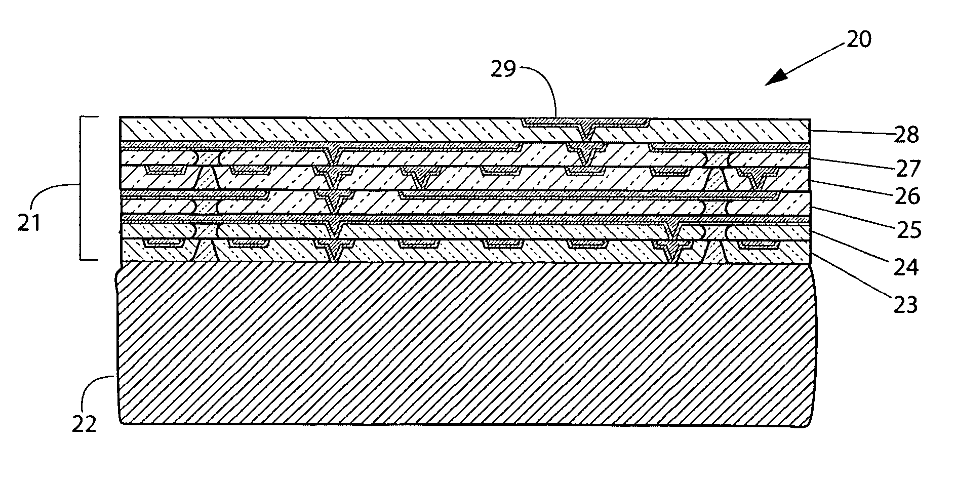
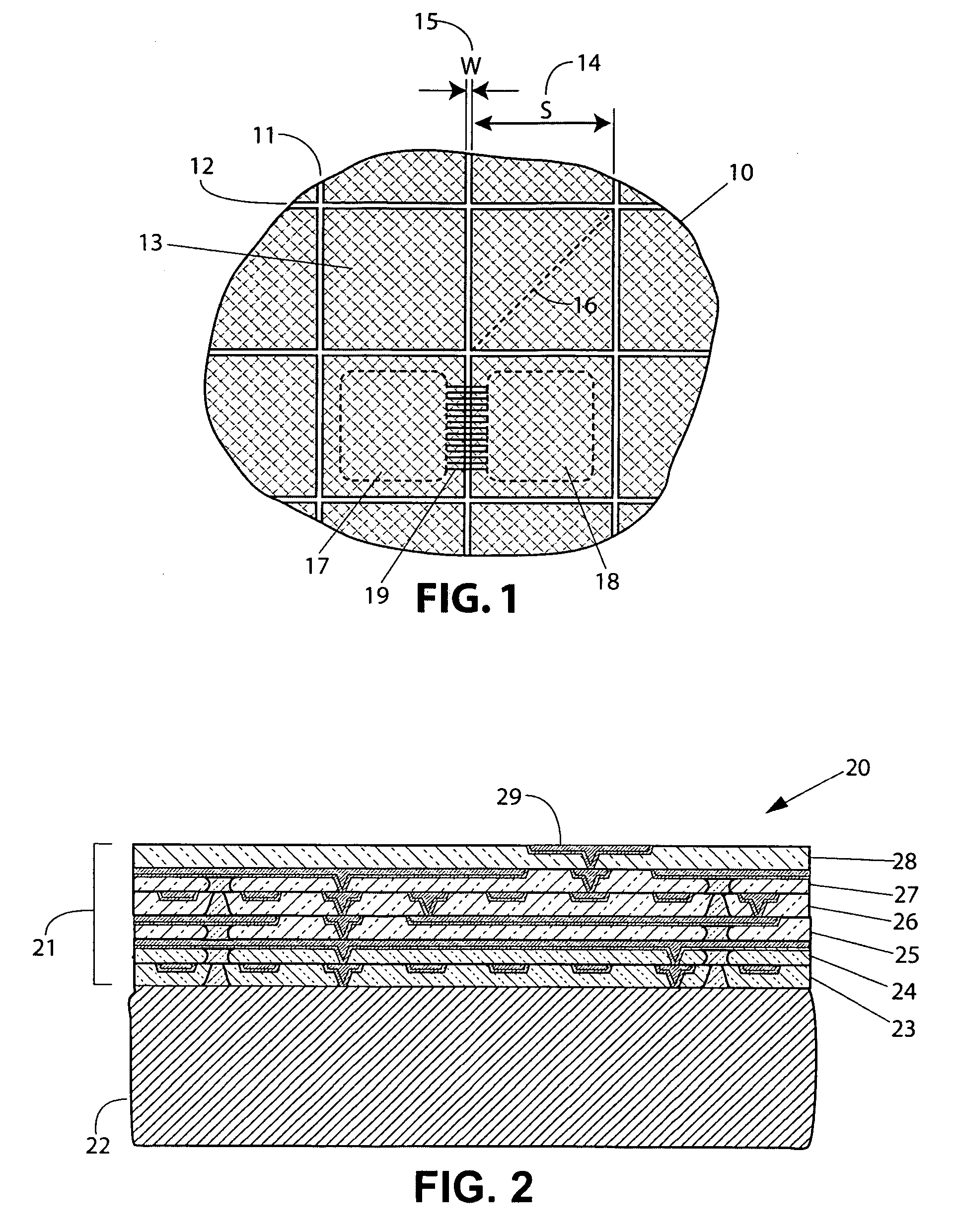
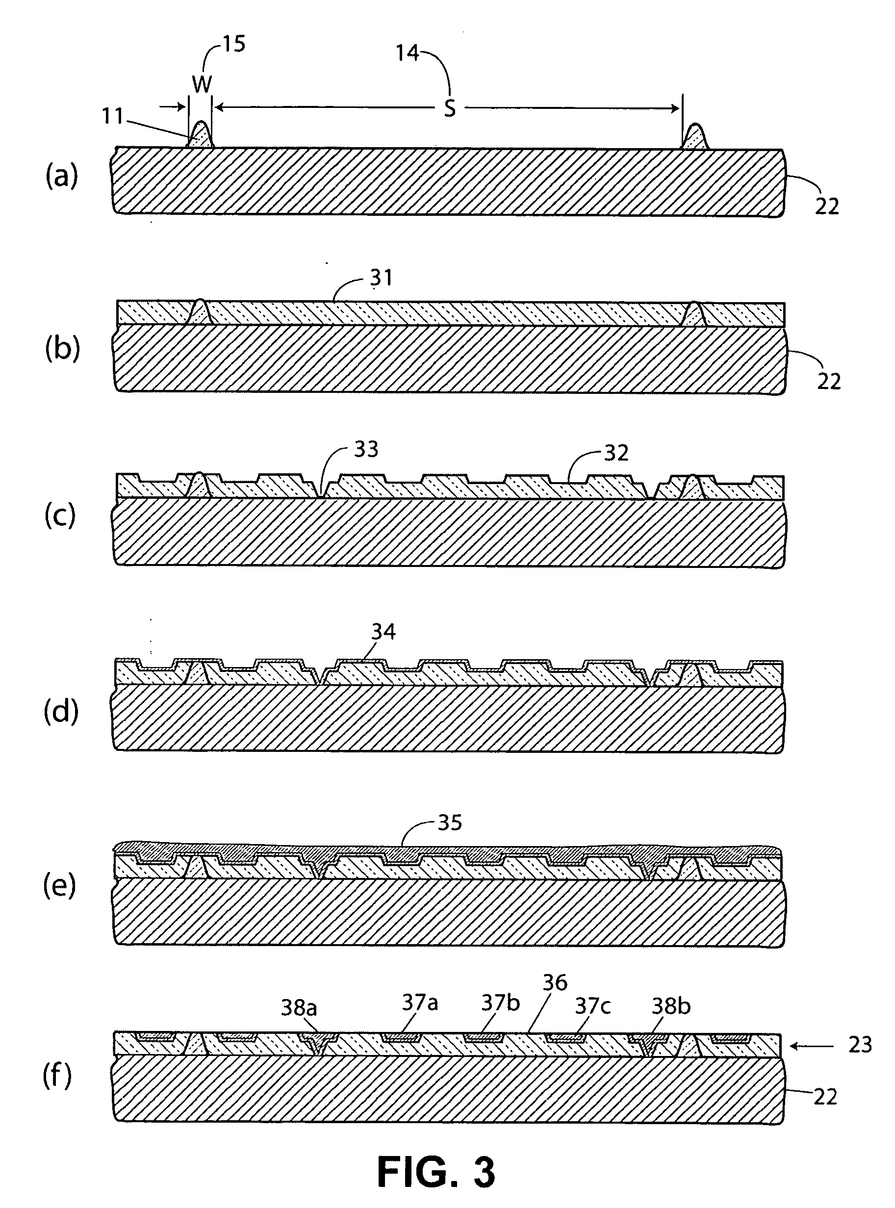
[0019] Various embodiments of the present invention are described hereinafter with reference to the figures. It should also be noted that the figures are only intended to facilitate the description of specific embodiments of the invention. They are not intended as an exhaustive description of the invention or as a limitation on the scope of the invention. In addition, an aspect described in conjunction with a particular embodiment of the present invention is not necessarily limited to that embodiment and can be practiced in any other embodiments of the present invention. For instance, in the following description, the tiled construction of the present invention is described with embodiments of low-k dielectric solutions. It will be appreciated that the claimed invention can be used not only for low-k dielectric solutions, but also any layered assembly wherein the elements are physically or thermally mismatched with each other, or with the substrate. These could include high-k dielec...


PUM


Abstract

A method is described for combining the diverse strengths of two materials in a tiled film construction. The first material provides a foundation of intersecting grid lines on a substrate and the second material is contained within the grid lines and has a valued property for a particular application. In a preferred embodiment, a tiled dielectric layer has improved low-k dielectric performance while avoiding film stress problems that can lead to delamination or cracking. CTE mismatch is overcome at the cost of an additional masking step. This tiling method and layered binary construction enable Cytop to be used as a high performance low-k dielectric on most substrates including semiconductor wafers and copper panels or foils.

Description

RELATED APPLICATIONS [0001] This application claims priority under 35 U.S.C. § 119(e) to Provisional Application Ser. No. 60 / 617,718 filed Oct. 12, 2004, the disclosure of which is hereby incorporated by reference in its entirety.BACKGROUND OF THE INVENTION [0002] 1. Field of the Invention [0003] This invention relates to methods for forming layers of binary material on substrates, and more particularly to high-performance dielectrics and methods of fabrication. [0004] 2. Description of the Related Art [0005] Layered constructions are well known for forming materials into useful composites. An example is a printed wiring board (PWB) with repeating layers of conductive traces embedded in dielectric material. A design problem occurs when a material has a desirable first property, but is disqualified in a particular application due to incompatibility with the substrate or an undesirable second property. For example, it will be shown that Cytop (an amorphous fluoropolymer) has exception...

Claims


Application Information

Patent Timeline
IPC IPC(8): H01L23/52
CPCH01L21/4857H01L23/49822H01L23/49838H01L23/49894H01L2924/3011H05K1/0271H05K1/056H05K3/107H05K3/465H05K2201/0187H01L2924/0002H01L2924/00
Inventor SALMON, PETER C.
Owner SALMON TECH
Why Eureka
Try Eureka