Designing method for high-frequency transistor and high-frequency transistor having multi-finger gate

Inactive Publication Date: 2006-05-18
SONY CORP
View PDF11 Cites 62 Cited by
  • Summary
  • Abstract
  • Description
  • Claims
  • Application Information

AI Technical Summary

Benefits of technology

[0025] According to another embodiment of the present invention, there is provided a high-frequency transistor having a multi-finger gate, including a transistor section having a source region and a drain region as well as a gate electrode having multi-fingers, all formed on a semiconductor substrate, a source wiring line connected to the source region, a drain wiring line connected to the drain region, and a gate wiring line connected to the gate electrode, the drain wiring line being disposed in an upper layer than that of the gate wiring line while a minimum dimension of a semiconductor fabrication process is applied to the dimension of a drain contact for connecting the drain wiring line to the drain region and the distance between the drain contact and the gate wiring line in order to reduce a coupling capacitance between the drain wiring line and the semiconductor substrate.
[0026] According to a further embodiment of the present invention, there is provided a high-frequency transistor having a multi-finger gate, including a transistor section having a source region and a drain region

Problems solved by technology

However, in design of a high-frequency transistor in related art having a finger gate, a pointer regarding what point should be taken notice of when the wiring line

Method used


Image

  • Designing method for high-frequency transistor and high-frequency transistor having multi-finger gate
  • Designing method for high-frequency transistor and high-frequency transistor having multi-finger gate
  • Designing method for high-frequency transistor and high-frequency transistor having multi-finger gate

Examples


structure example 1

[0230] In the method of designing a high-frequency transistor according to the present embodiment, in order to reduce the coupling capacitance between the drain wiring line and the gate wiring line and the coupling capacitance between the drain wiring line and the substrate without changing the transistor size, preferably the drain wiring line is formed in an upper layer with respect to the gate wiring line (structure example 1).

[0231]FIG. 18 is a sectional view of the structure example 1. In this instance, the plane pattern itself can be designed similarly as in FIG. 15. In particular, in FIG. 18, the portion 6A in the form of a rectangular framework of the gate wiring line is formed from the 1MT, and the intermediate connection layer 4 and the second gate contact 5 (FIG. 16) are omitted while the first gate contact 3 is used to connect the increased width portion of the gate electrode 2 for connecting the finger portions F and the portion 6A in the form of a rectangular framework...

structure example 2

[0234]FIG. 19 shows a sectional view of a high-frequency transistor of the structure example 2 taken along a line same as the B-B line of FIG. 15.

[0235] In the structure example 2, in addition to the formation of the drain wiring line 7 as an upper layer than that of the gate wiring line 6, the contact portion of the drain region is optimized.

[0236] More particularly, the drain wiring line 7 formed from the 2MT is connected to the drain region DR formed on the semiconductor substrate 1 by a deep drain contact 8. The drain region DR is formed on the semiconductor substrate 1 by ion implantation performed using two adjacent finger portions F as a mask layer. The diameter of the deep drain contact 8 has a minimum dimension Wc relating to a contact of a semiconductor fabrication process used for the formation of the transistor. Meanwhile, the distance from the deep drain contacts 8 to the finger portions F is a minimum dimension Wc_c relating to the distance between a contact and anot...

structure example 3

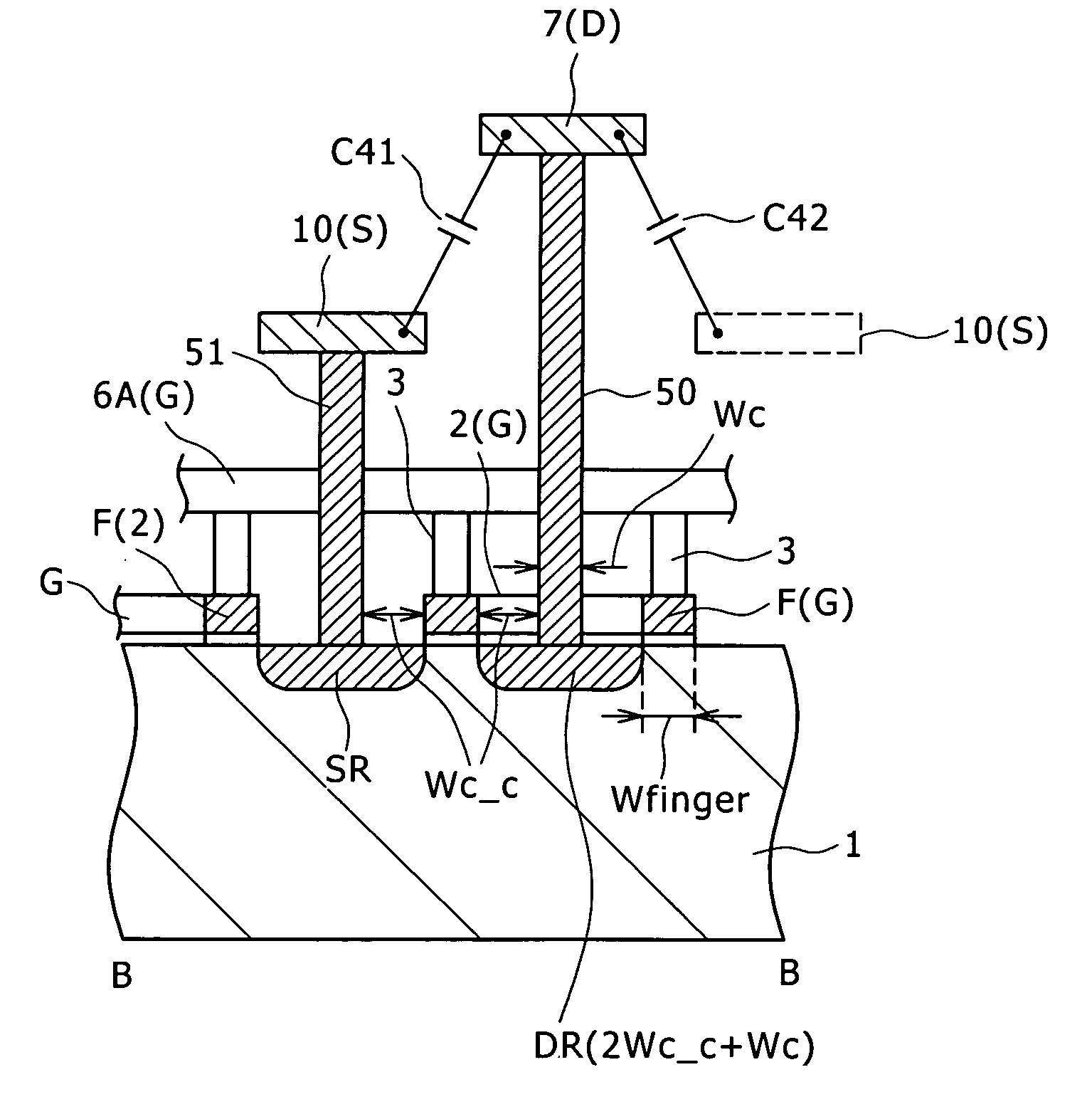
[0237] In the structure example 1 and the structure example 2, only it is necessary for the drain wiring line 7 to be formed as an upper layer than the gate wiring line 6, and such modification that the drain wiring line 7 is placed on a layered level higher than the third layer metal (3MT) is possible.

[0238] The structure example 3 is a modification to the structure example 2 in that the drain wiring line 7 is formed from the 3MT, and a sectional view thereof is shown in FIG. 20.

[0239] In the structure example 3, the coupling capacitances C41 and C42 between the drain wiring lines 7 and the source wiring line 10 are smaller than those in the case of FIG. 16. Therefore, there is the possibility that the high-frequency characteristics of the transistor of the structure example 3 may be further improved when compared with the structure example 1.

[0240] The present invention can be applied to a high-frequency transistor model which is incorporated in and used with such software as t...


PUM


Abstract

The present invention provides a designing method for a high-frequency transistor, which includes a transistor section, a drain region, and a gate electrode, a source wiring line, a drain wiring line, and a gate wiring line, for optimizing wiring lines and contacts from voltage supplying nodes to electrode lead nodes. The method includes the steps of measuring a sensitivity to a high-frequency characteristic of the high-frequency transistor regarding coupling capacities between the wiring lines and coupling capacities between the wiring lines and the semiconductor substrate from among equivalent circuit parameters which vary in response to a configuration of the wiring lines and the contacts; deciding layered levels individually of the gate wiring line, source wiring line, and drain wiring line based on the measured sensitivities; and designing patterns of the gate wiring line, source wiring line, and drain wiring line in the individually decided layered levels and the positions and the sizes of the wiring lines and the contacts for connecting the wiring lines and the transistor section to each other.

Description

CROSS REFERENCES TO RELATED APPLICATIONS [0001] The present invention contains subject matter related to Japanese Patent Application JP 2004-334267 filed in the Japanese Patent Office on Nov. 18, 2004, the entire contents of which being incorporated herein by reference. BACKGROUND OF THE INVENTION [0002] This invention relates to a designing method for a high-frequency transistor for optimizing wiring lines to electrode lead nodes and contacts of a transistor unit of a high-frequency semiconductor circuit and a high-frequency transistor having a multi-finger gate. [0003] In recent years, it has become possible to obtain, in fine CMOS techniques, a characteristic of a current gain cutoff frequency ft which exceeds 100 GHz. Therefore, a CMOS transistor has begun to be used for high-frequency communication by a wireless LAN, the Bluetooth, or the like in place of an MESFET or a bipolar transistor in related art for which 3-5 group semiconductors (GaAs, InP) are used. [0004] For the CMO...

Claims


Application Information

Patent Timeline
IPC IPC(8): G06F17/50
CPCG06F17/5063G06F30/36
Inventor NAKAMURA, AKIHIRO
Owner SONY CORP
Why Eureka
Try Eureka