Barrier material and process for Cu interconnect

a barrier material and interconnection technology, applied in the direction of semiconductor devices, semiconductor/solid-state device details, electrical apparatus, etc., can solve the problems of limiting device performance, signal propagation delay caused, copper may not be deposited in higher amounts in an efficient manner, etc., to achieve the effect of improving electromigration performan

Inactive Publication Date: 2006-06-01
TAIWAN SEMICON MFG CO LTD
View PDF17 Cites 571 Cited by
  • Summary
  • Abstract
  • Description
  • Claims
  • Application Information

AI Technical Summary

Benefits of technology

[0010] These and other problems are generally solved or circumvented, and technical advantages are generally achieved, by preferred embodiments of the present invention, in which improved structures and methods relating to copper diffusion barriers yield devices having enhanced electromigration performance.

Problems solved by technology

In integrated circuits having minimum dimensions of approximately 0.35 μm and less, a limiting factor of device performance is the signal propagation delay caused by the switching speed of the transistor elements.
As the channel length of these transistor elements has now reached 0.18 μm and less, however, capacitance between neighboring conductive structures is increasingly problematic.
For example, copper may not be deposited in higher amounts in an efficient manner by well-established deposition methods, such as chemical and physical vapor deposition.
Moreover, copper may not be efficiently patterned by well-established anisotropic etch processes and therefore the so-called damascene technique is employed in forming metallization layers including copper lines.
A further issue is the ability of copper to readily diffuse in silicon dioxide.
Therefore, copper diffusion may negatively affect device performance, or may even lead to a complete failure of the device.
Although copper exhibits superior characteristics with respect to resistance to electromigration compared to aluminum, the ongoing shrinkage of feature sizes, however, leads to increased current densities, thereby causing a non-acceptable degree of electromigration.
This can produce voids in the copper lines that may cause device failure.
As previously noted, the device performance of extremely scaled integrated circuits is substantially limited by the parasitic capacitances of adjacent interconnect lines, which may be reduced by decreasing the resistivity thereof and by decreasing the capacitive coupling in that the overall dielectric constant of the dielectric layer is maintained as low as possible.
It turns out, however, that the barrier characteristics of the silicon nitride layer depend on the thickness thereof so that thinning the silicon nitride layer, as would be desirable for a reduced overall dielectric constant, may not be practical to an extent as required for further scaling semiconductor devices including copper metallization layers without compromising device performance.

Method used


Image

  • Barrier material and process for Cu interconnect
  • Barrier material and process for Cu interconnect
  • Barrier material and process for Cu interconnect

Examples


Embodiment Construction

[0026] The operation and fabrication of the presently preferred embodiments are discussed in detail below. However, the embodiments and examples described herein are not the only applications or uses contemplated for the invention. The specific embodiments discussed are merely illustrative of specific ways to make and use the invention, and do not limit the scope of the invention or the appended claims.

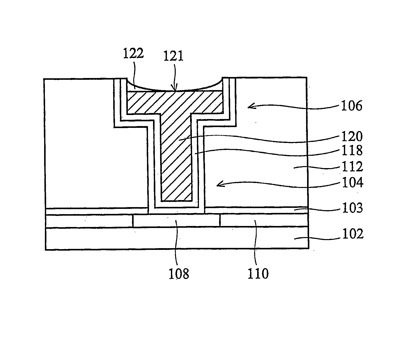
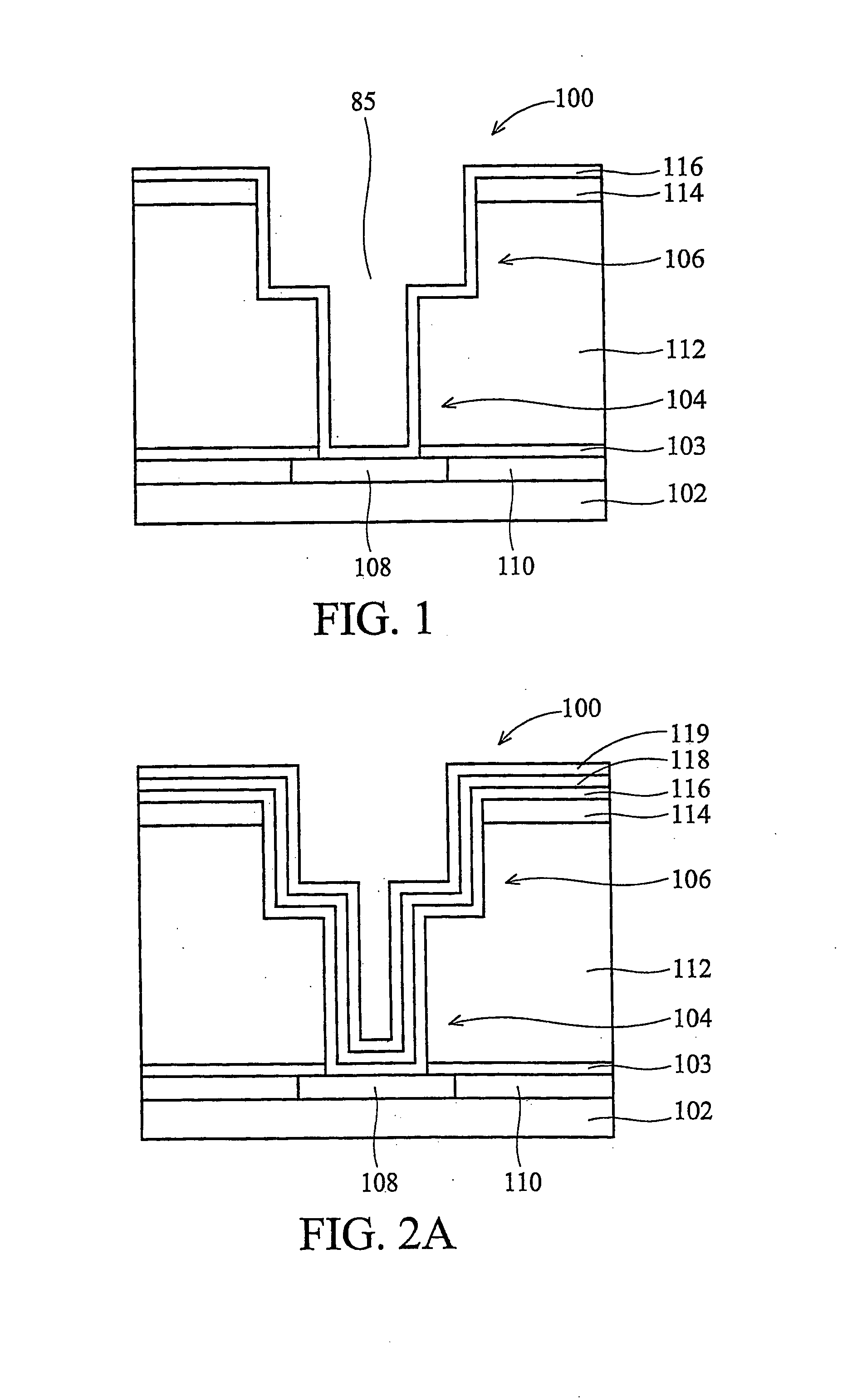
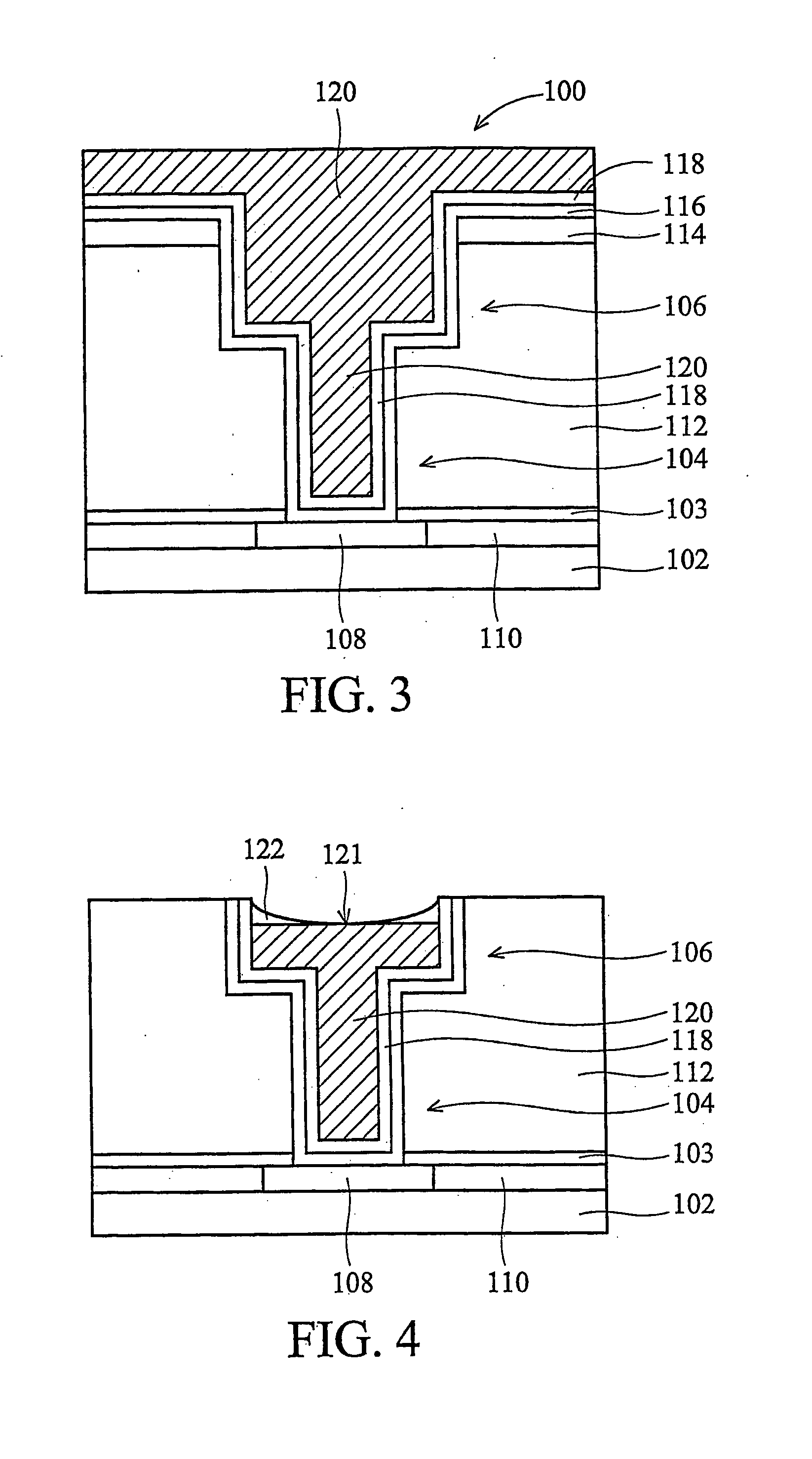
[0027] This invention relates generally to semiconductor device fabrication and more particularly to a structure and method for improved resistance to electromigration problems with conductive lines and vias, such as copper, between interconnected layers. The present invention will now be described with respect to preferred embodiments in a specific context, namely the creation of copper conductive lines and vias in the damascene process. It is believed that embodiments of this invention are particularly advantageous when used in this process. It is further believed that embodiments ...


PUM

PropertyMeasurementUnit
thicknessaaaaaaaaaa
channel lengthaaaaaaaaaa
dielectric constantaaaaaaaaaa

Abstract

A semiconductor diffusion barrier layer and its method of manufacture is described. The barrier layer includes of at least one layer of TaN, TiN, WN, TbN, VN, ZrN, CrN, WC, WN, WCN, NbN, AlN, and combinations thereof. The barrier layer may further include a metal rich surface. Embodiments preferably include a glue layer about 10 to 500 Angstroms thick, the glue layer consisting of Ru, Ta, Ti, W, Co, Ni, Al, Nb, AlCu, and a metal-rich nitride, and combinations thereof. The ratio of the glue layer thickness to the barrier layer thickness is preferably about 1 to 50. Other alternative preferred embodiments further include a conductor annealing step. The various layers may be deposited using PVD, CVD, PECVD, PEALD and/or ALD methods including nitridation and silicidation methods.

Description

TECHNICAL FIELD [0001] This invention relates generally to semiconductor device fabrication and more particularly to a structure and method for improved resistance to electromigration problems with conductive lines and vias, such as copper, between interconnected layers. BACKGROUND [0002] In modern integrated circuits, minimum feature sizes, such as the channel length of field effect transistors, have reached the deep sub-micron range, thereby steadily increasing performance of these circuits in terms of speed and power consumption. As the size of the individual circuit elements is reduced, so is the available real estate for conductive interconnects in integrated circuits. Consequently, these interconnects have to be reduced to compensate for a reduced amount of available real estate and for an increased number of circuit elements provided per chip. [0003] In integrated circuits having minimum dimensions of approximately 0.35 μm and less, a limiting factor of device performance is ...

Claims


Application Information

Patent Timeline
Patent Type & Authority Applications(United States)
IPC IPC(8): H01L21/44H01L23/48
CPCH01L21/76814H01L21/76825H01L2924/0002H01L21/76826H01L21/76834H01L21/76846H01L21/76849H01L21/76864H01L21/76873H01L21/76877H01L21/76883H01L23/53238H01L23/5329H01L23/53295H01L2221/1089H01L2924/00
Inventor CHANG, CHUNG-LIANGHSIEH, CHING-HUASHUE, SHAU-LIN
Owner TAIWAN SEMICON MFG CO LTD
Why Eureka
Try Eureka