Semiconductor device including a porous low-k material layer stack with reduced UV sensitivity

a low-k material, uv-sensitive technology, applied in the direction of solid-state devices, basic electric elements, electric apparatus, etc., can solve the problems of increasing production yield, signal propagation delay no longer limited, density and mechanical stability or strength of low-k materials may be significantly less, etc., to reduce the penetration of dielectric barrier materials, increase the porosity of low-k dielectric materials, and high degree of flexibility in selecting

Inactive Publication Date: 2008-05-01
GLOBALFOUNDRIES INC
View PDF7 Cites 19 Cited by
  • Summary
  • Abstract
  • Description
  • Claims
  • Application Information

AI Technical Summary

Benefits of technology

[0014]Generally, the subject matter disclosed herein relates to a techniques for forming a sophisticated low-k dielectric layer stack wherein the low-k dielectric material may be subjected to a radiation treatment to increase the porosity of the low-k dielectric material. Contrary to conventional approaches, in which a high degree of flexibility in selecting respective porogen materials is desired, the influence of the corresponding radiation treatment on the underlying dielectric barrier layer may be significantly reduced by providing a respective radiation blocking cap layer which may significantly reduce the penetration of the dielectric barrier material by incident radiation. Consequently, significant changes in material characteristics, such as a reduction of compressive stress which may advantageously be generated in the dielectric barrier layer for enhancing mechanical stability and enhancing electromigration performance of the entire layer stack, may be substantially maintained. Furthermore, by providing highly reflective and / or absorbing materials on the dielectric barrier layer, the corresponding layer thickness may be selected moderately thin, thereby also reducing any adverse effect of the corresponding cap layer with respect to the overall permittivity of the low-k dielectric layer stack.

Problems solved by technology

Thus, economic constraints drive semiconductor manufacturers to steadily increase the substrate dimensions, thereby also increasing the area available for producing actual semiconductor devices and thus increasing production yield.
For extremely scaled integrated circuits, the signal propagation delay is no longer limited by the circuit elements, for instance by field effect transistors, but is limited, owing to the increased density of circuit elements, which requires an even more increased number of electrical connections, by the close proximity of the metal lines, since the line-to-line capacitance increases as the spacing decreases.
However, the density and mechanical stability or strength of the low-k materials may be significantly less compared to the well-approved dielectrics silicon dioxide and silicon nitride.
As a consequence, the electrical behavior of the metallization layers, although being superior in view of device performance, may be inferior with respect to reliability and also with respect to substrate handling and transport, as explained above, compared to devices having a conventional metallization layer.
Therefore, the metallization level may represent a delicate structure, in which diverging requirements with respect to electrical performance and reliability and stability have to be precisely balanced.
For example, for a thermal treatment, a reduced number of porogen materials is currently available, thereby also restricting the compatibility with subsequent process steps.
It turns out, however, that the characteristics of the resulting layer stack and in particular of the barrier layer 105 may result in reduced performance and / or stability when the treatment 108 includes UV irradiation.

Method used


Image

  • Semiconductor device including a porous low-k material layer stack with reduced UV sensitivity
  • Semiconductor device including a porous low-k material layer stack with reduced UV sensitivity
  • Semiconductor device including a porous low-k material layer stack with reduced UV sensitivity

Examples


Embodiment Construction

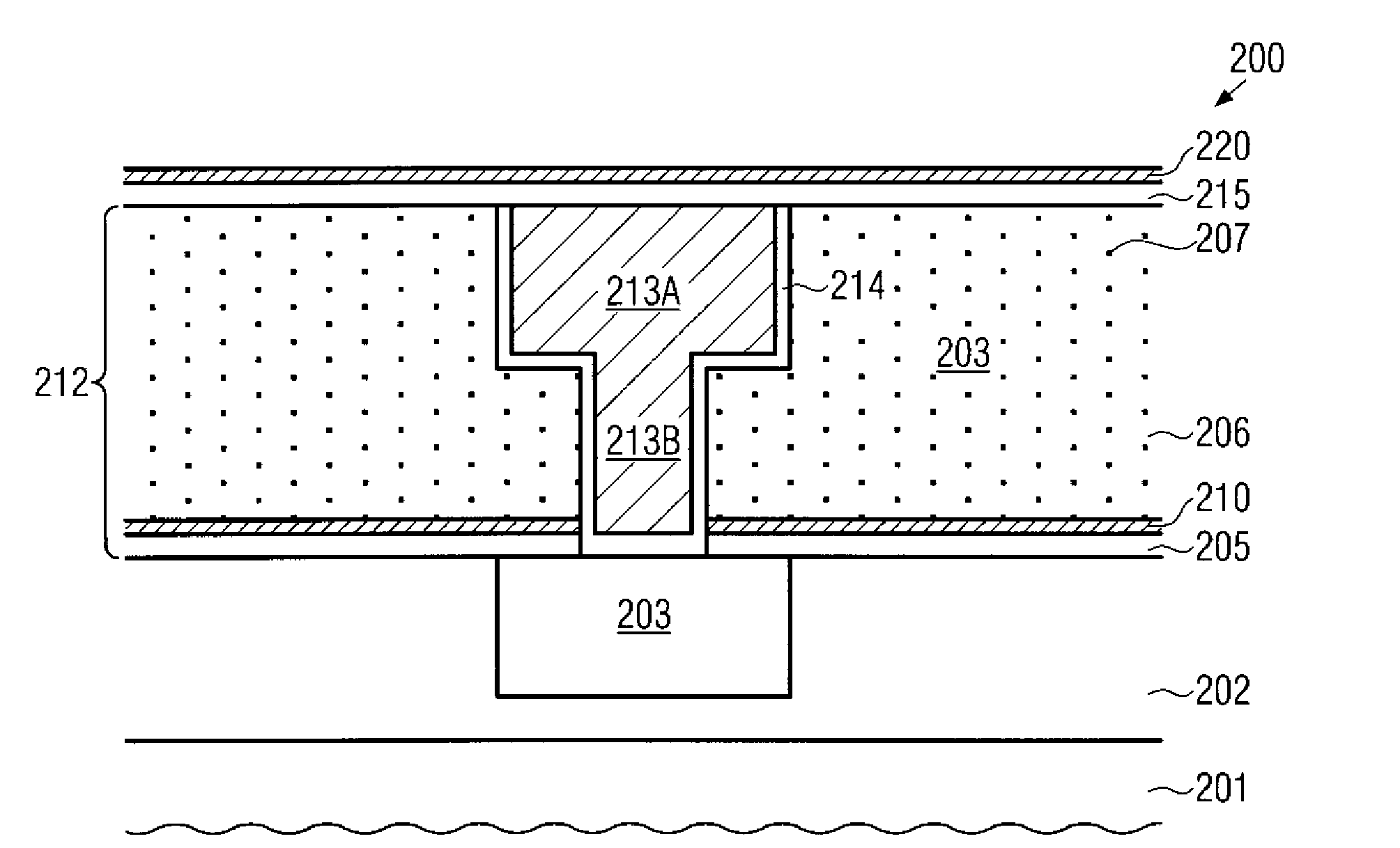
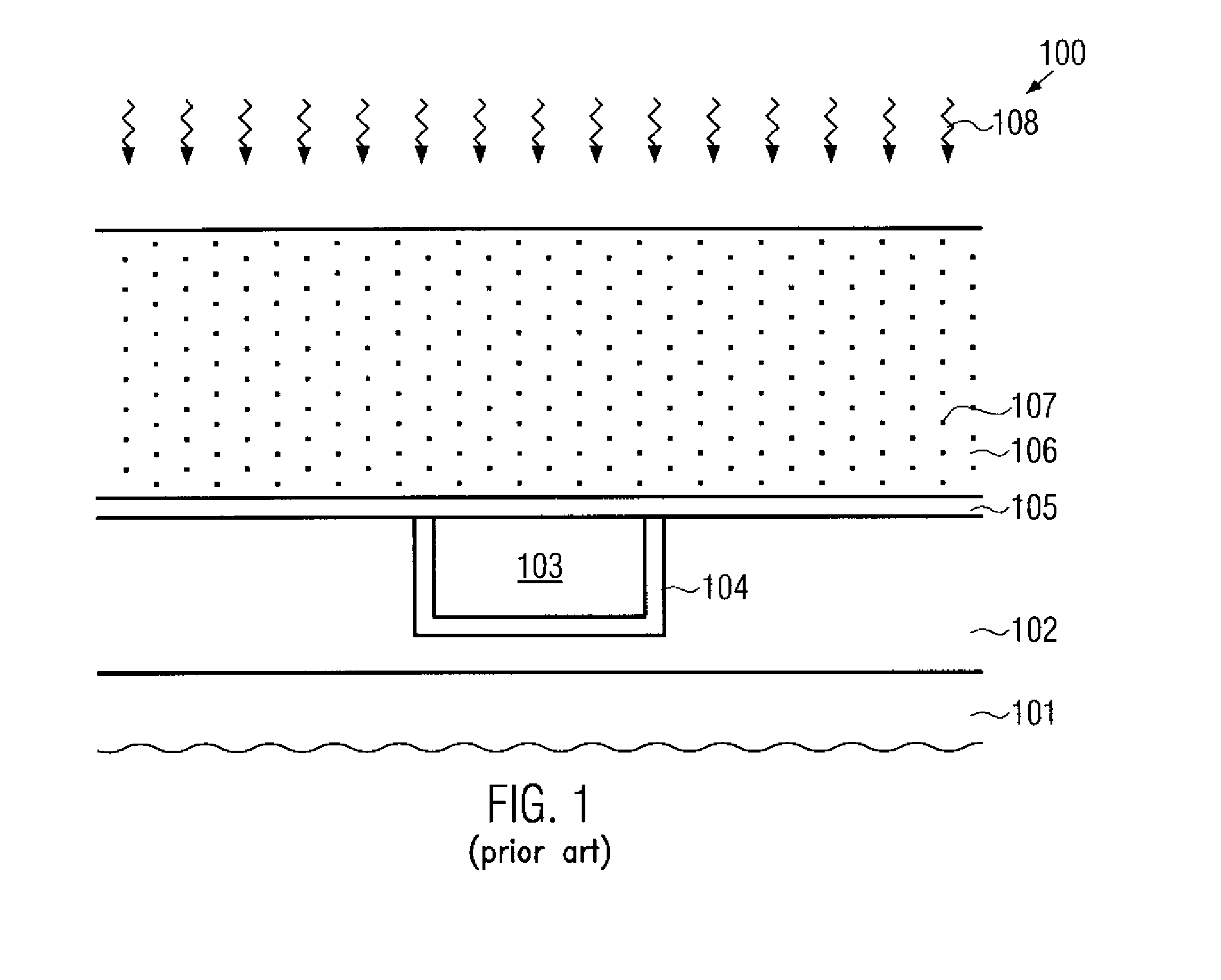
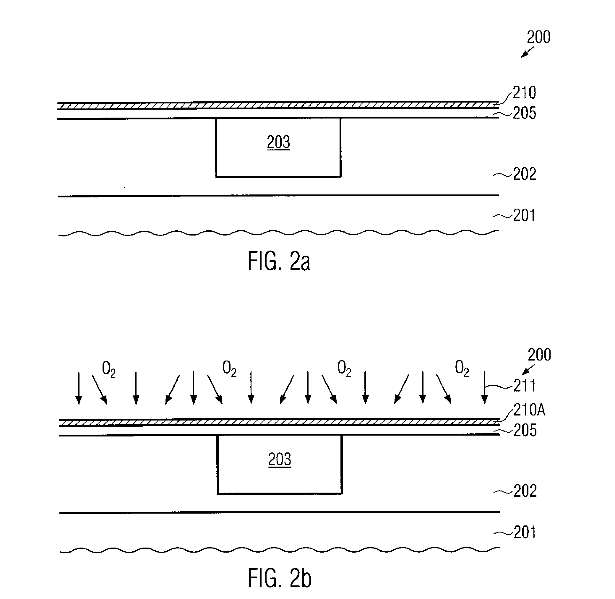
[0023]Various illustrative embodiments of the invention are described below. In the interest of clarity, not all features of an actual implementation are described in this specification. It will of course be appreciated that in the development of any such actual embodiment, numerous implementation-specific decisions must be made to achieve the developers' specific goals, such as compliance with system-related and business-related constraints, which will vary from one implementation to another. Moreover, it will be appreciated that such a development effort might be complex and time-consuming, but would nevertheless be a routine undertaking for those of ordinary skill in the art having the benefit of this disclosure.

[0024]The present subject matter will now be described with reference to the attached figures. Various structures, systems and devices are schematically depicted in the drawings for purposes of explanation only and so as to not obscure the present disclosure with details ...


PUM

PropertyMeasurementUnit
thicknessaaaaaaaaaa
relative permittivityaaaaaaaaaa
gate lengthaaaaaaaaaa

Abstract

By forming a cap layer on a dielectric barrier layer of a low-k dielectric material stack, the interaction of UV radiation during the generation of pores in the low-k dielectric material may be significantly reduced. In some illustrative embodiments, the cap layer may comprise titanium oxide and/or vanadium oxide which may provide a high degree of reflectivity and absorption, respectively. The layer thickness of the cap layer may be 10 nm or significantly less, thereby reducing any adverse influence on the overall performance of the resulting layer stack.

Description

BACKGROUND OF THE INVENTION[0001]1. Field of the Invention[0002]Generally, the present disclosure relates to the fabrication of integrated circuits, and, more particularly, to the formation of metallization layers of reduced permittivity including porous low-k dielectric materials and advanced dielectric barrier layers.[0003]2. Description of the Related Art[0004]Semiconductor devices are typically formed on substantially disc-shaped substrates made of any appropriate material. The majority of semiconductor devices including highly complex electronic circuits are currently, and in the foreseeable future will be, manufactured on the basis of silicon, thereby rendering silicon substrates and silicon-containing substrates, such as silicon-on-insulator (SOI) substrates, viable carriers for forming semiconductor devices, such as microprocessors, SRAMs, ASICs (application specific ICs) and the like. The individual integrated circuits are arranged in an array form, wherein most of the manu...

Claims


Application Information

Patent Timeline
Patent Type & Authority Applications(United States)
IPC IPC(8): H01L23/52H01L21/31
CPCH01L21/3105H01L21/31683H01L21/7682H01L21/76832H01L23/53295H01L21/76856H01L23/53238H01L23/5329H01L21/76834H01L2924/0002H01L2221/1047H01L21/02266H01L21/02175H01L21/02203H01L21/02271H01L21/02167H01L2924/00H01L21/02348H01L21/02362
Inventor STRECK, CHRISTOFKAHLERT, VOLKER
Owner GLOBALFOUNDRIES INC
Why Eureka
Try Eureka