
Method of manufacturing silicon optoelectronic device, silicon optoelectronic device manufacture by the method, and image input and/or output apparatus using the silicon optoelectronic device

a manufacturing method and optoelectronic technology, applied in the direction of sustainable manufacturing/processing, instruments, radiation control devices, etc., can solve the problems of difficult to control the size of nano-crystal silicon quantum dots, low light-emitting efficiency, and low cost. , to achieve the effect of excellent light-emitting efficiency and high wavelength selectivity

Inactive Publication Date: 2006-06-01
SAMSUNG ELECTRONICS CO LTD
View PDF52 Cites 20 Cited by
  • Summary
  • Abstract
  • Description
  • Claims
  • Application Information

AI Technical Summary

Benefits of technology

[0019] The present invention provides a method of manufacturing a silicon optoelectronic device which has excellent light-emitting efficiency, can be used as at least one of a light-emitting device and a light-receiving device, and has high wavelength selectivity. The present invention also provides a silicon optoelectronic device manufactured by the method and an image input and / or output apparatus used the silicon optoelectronic device.
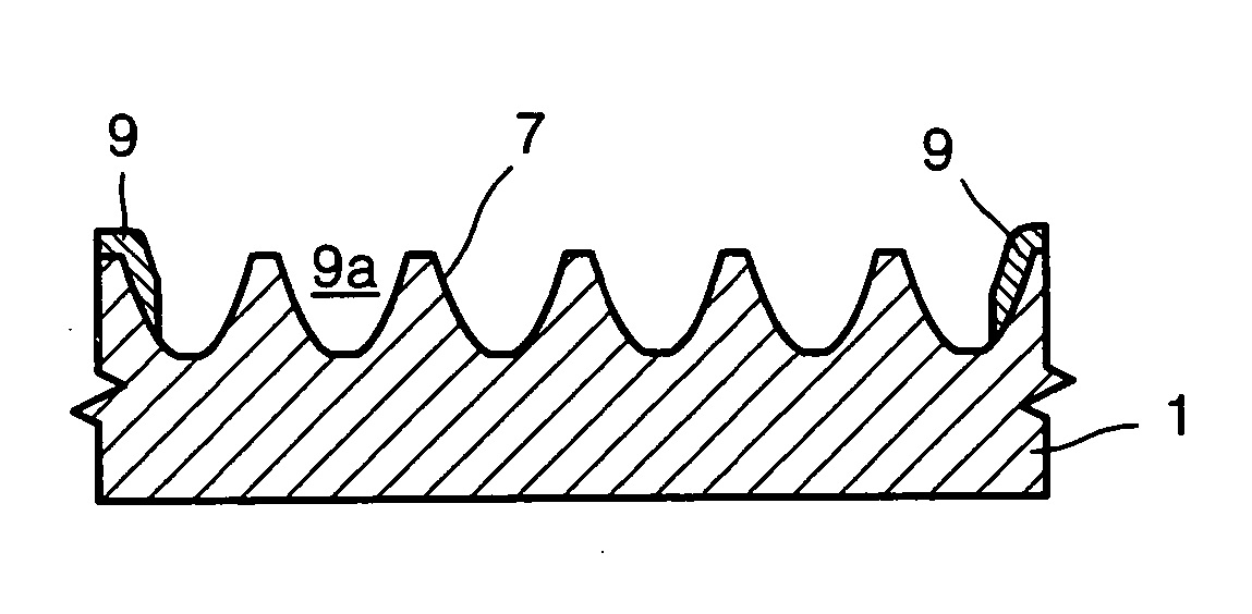
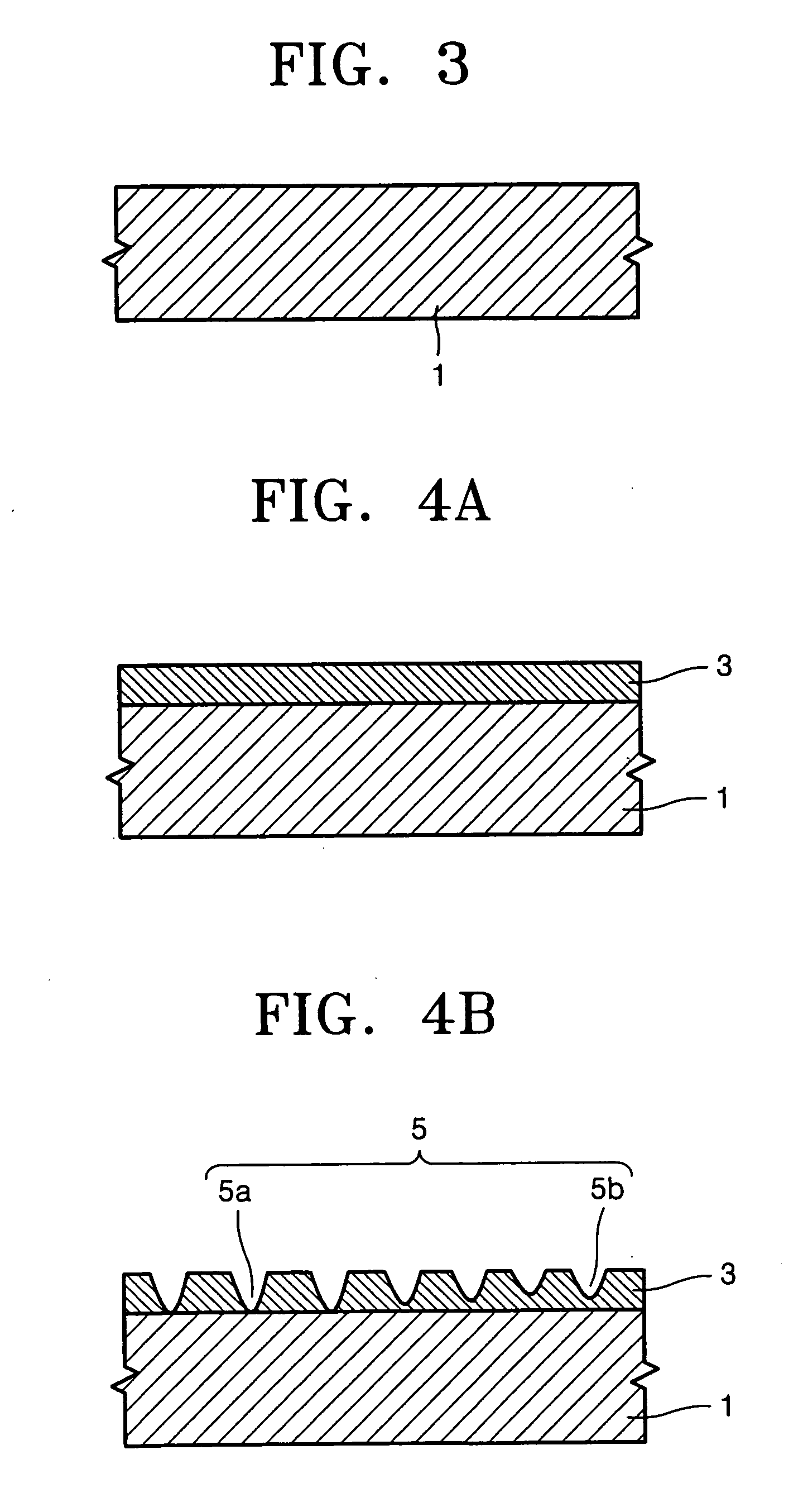
[0020] According to an aspect of the present invention, there is provided a method of manufacturing a silicon optoelectronic device comprising: preparing an n- or p-type silicon-based substrate; forming a microdefect pattern along a surface of the substrate by etching; forming a control film with an opening on the microdefect pattern; and forming a doping region on the surface of the substrate having the microdefect pattern in such a way that a predetermined dopant of the opposite type to the substrate is injected onto the substrate through the opening of the control film to be doped to a depth so that a photoelectric conversion effect leading to light emission and / or reception by quantum confinement effect in a p-n junction occurs.

Problems solved by technology

However, a porous silicon based light-emitting device as described above does not yet provide reliability as a light-emitting device and exhibits external quantum efficiency (EQE) as low as 0.1%.
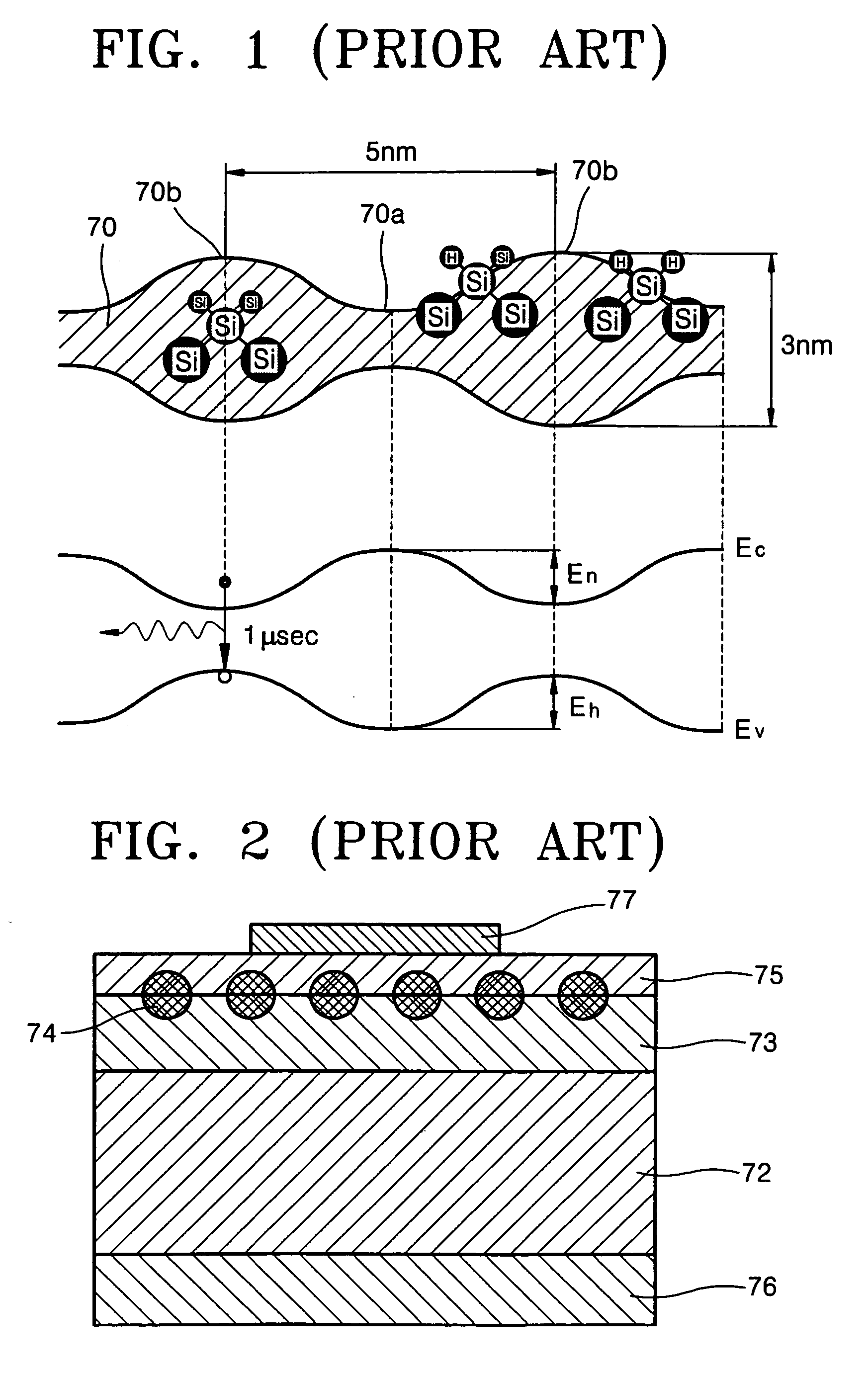
However, light-emitting devices using the nano-crystal silicon quantum dots 74 have problems in that it is difficult to control the sizes of the nano-crystal silicon quantum dots and to obtain the uniformity of the nano-crystal silicon quantum dots, and light-emitting efficiency is very low.

Method used


Image

  • Method of manufacturing silicon optoelectronic device, silicon optoelectronic device manufacture by the method, and image input and/or output apparatus using the silicon optoelectronic device
  • Method of manufacturing silicon optoelectronic device, silicon optoelectronic device manufacture by the method, and image input and/or output apparatus using the silicon optoelectronic device
  • Method of manufacturing silicon optoelectronic device, silicon optoelectronic device manufacture by the method, and image input and/or output apparatus using the silicon optoelectronic device

Examples


first embodiment

[0125]FIG. 16 is a schematic plan view of an image input and / or output apparatus according to the present invention.

[0126] Referring to FIGS. 12 and 16, an image input and / or output apparatus according to the first embodiment of the present invention comprises a silicon optoelectronic device panel 25 having a two-dimensional array of silicon optoelectronic devices 20, each of which leads to input and / or output of an image, formed on an n- or p-type silicon-based substrate 1. The term, “image output” as used herein indicates substantially an image display. The term, “image input” as used herein indicates substantially generation of an electric image signal of an object photographed using a camera. The silicon optoelectronic devices 20 are described in the above, and thus, the overlapped descriptions thereof will be omitted.

[0127] As described above, each of the silicon optoelectronic devices 20 can be used as a light emitting and / or receiving device of a specific wavelength band or ...

third embodiment

[0141]FIG. 19 is a schematic view of an image input and / or output image apparatus according to the present invention.

[0142] In an image input and / or output apparatus according to the third embodiment of the present invention, the silicon optoelectronic device panel 40 is designed in such a way that three or more silicon optoelectronic devices correspond to each pixel P. FIG. 19 shows an example of the silicon optoelectronic device panel 40 having three silicon optoelectronic devices 20R, 20G, and 20B per each pixel P.

[0143] In this case, the three silicon optoelectronic devices 20R, 20G, and 20B corresponding to each pixel P output and / or absorb red light R, green light G, and blue light B (for example), respectively and then convert the detected color light into respective electrical color image signals. The three silicon optoelectronic devices 20R, 20G, and 20B have microdefect patterns of different periods corresponding to specific wavelength bands, for example, red light R, gre...


PUM

PropertyMeasurementUnit
thicknessaaaaaaaaaa
thicknessaaaaaaaaaa
EQEaaaaaaaaaa

Abstract

A method of manufacturing a silicon optoelectronic device, a silicon optoelectronic device manufactured by the method, and an image input and / or output apparatus including the silicon optoelectronic device are provided. The method includes preparing an n- or p-type silicon-based substrate, forming a microdefect pattern along a surface of the substrate by etching, forming a control film with an opening on the microdefect pattern, and forming a doping region on the surface of the substrate having the microdefect pattern in such a way that a predetermined dopant of the opposite type to the substrate is injected onto the substrate through the opening of the control film to be doped to a depth so that a photoelectric conversion effect leading to light emission and / or reception by quantum confinement effect in the p-n junction occurs. The silicon optoelectronic device has superior light-emitting efficiency, can be used as at least one of a light-emitting device and a light-receiving device, and has high wavelength selectivity. In addition, the silicon optoelectronic device panel having the two-dimensional array of the silicon optoelectronic devices can be applied in the image input and / or output apparatus capable of directly displaying an image and / or inputting optical information in a screen.

Description

BACKGROUND OF THE INVENTION [0001] This application claims the priority from Korean Patent Application No. 2003-3259, filed on Jan. 17, 2003, in the Korean Intellectual Property Office, the disclosure of which is incorporated herein in its entirety by reference. [0002] 1. Field of the Invention [0003] The present invention relates to a method of manufacturing a silicon optoelectronic device, a silicon optoelectronic device manufactured by the method, and an image input and / or output apparatus having the silicon optoelectronic device. [0004] 2. Description of the Related Art [0005] An advantage of using a silicon semiconductor substrate is that it provides excellent reliability and allows highly integrated density of a logic device, an operation device, and a drive device on the substrate. Also, a silicon semiconductor material can be used in fabrication of a highly integrated circuit at much lower cost than a compound semiconductor material, due to the use of inexpensive silicon. Th...

Claims


Application Information

Patent Timeline
Patent Type & Authority Applications(United States)
IPC IPC(8): H01L21/00H01L27/146H01L27/15H01L31/10H01L31/12H01L33/06H01L33/08H01L33/34
CPCB82Y10/00B82Y20/00B82Y30/00G01Q80/00H01L27/14601H01L27/14621H01L27/14645H01L27/14683H01L27/156H01L31/0236H01L31/028H01L31/035281H01L31/1804H01L33/0054H01L33/24H01L33/34Y02E10/547H01L31/02363Y02P70/50H01L31/12
Inventor LEE, EUN-KYUNGCHOI, BYOUNG-IYONGAHN, PIL-SOOKIM, JUN-YOUNGJIN, YOUNG-GU
Owner SAMSUNG ELECTRONICS CO LTD
Learn More