Manufacturing process for annealed wafer and annealed wafer

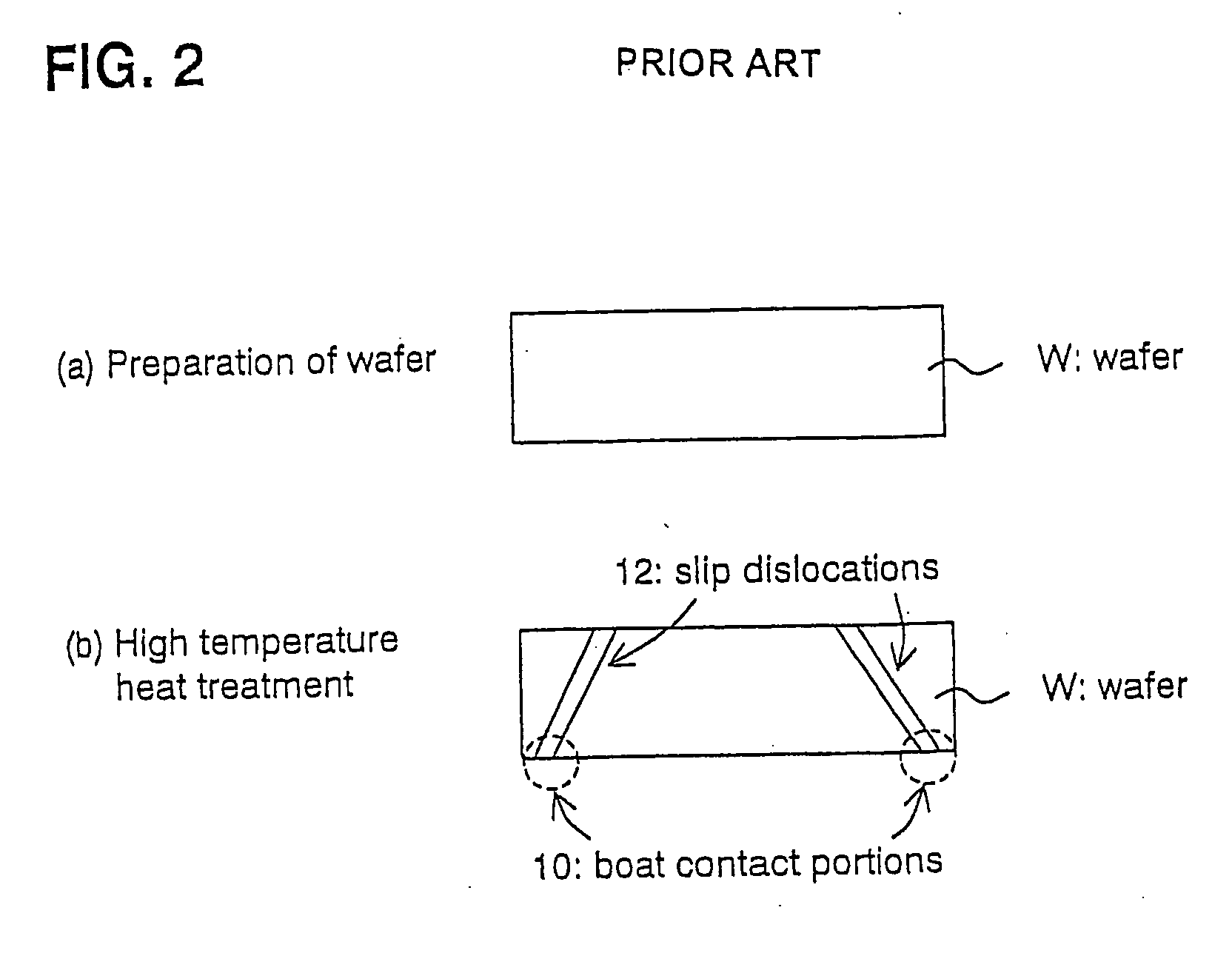
a manufacturing process and technology of annealing wafer, applied in the direction of crystal growth process, electrical apparatus, basic electric elements, etc., can solve the problems of large slip dislocation (long slip dislocation in length) generated remarkably, and cannot avoid the slip dislocation by modifying the shape of the boat, so as to achieve large stress, increase the weight of the wafer itself, and increase the effect of diameter

Inactive Publication Date: 2006-06-08
SHIN-ETSU HANDOTAI CO LTD
View PDF7 Cites 3 Cited by
  • Summary
  • Abstract
  • Description
  • Claims
  • Application Information

AI Technical Summary

Benefits of technology

[0008] The reason for the above could conceivably include the following points. A weight of a wafer itself increases greatly with increase in diameter thereof from 200 mm to 300 mm, which causes a large stress to be imposed on contact portions of the wafer with the boat. There has become normally used such a wafer as its diameter increases by a factor of 1.5, but its thickness increases only by a factor of 1.1 or less (for example, a thickness of 725 μm for a 200 mm wafer and a thickness of 775 μm for a 300 mm wafer), so that a resistance to slip dislocations decreases. A larger diameter increases a temperature difference across a wafer surface during temperature increase and decrease in heat treatment.
[0009] It has been generally known that when thermal stress is given to a silicon wafer containing oxide precipitates, slip dislocations may be generated from the oxide precipitates themselves, and for example, in JP A 98-150048, there are described findings that in the case where oxide precipitates are polyhedral precipitates or plate-like precipitates, when the sizes thereof become not less than about 200 nm or about 230 nm, respectively, slip dislocations are generated easily.
[0011] The present invention was made in order to solve the above problem and it is an object of the present invention to provide a heat-treating method capable of suppressing generation of slip dislocations in a CZ silicon single crystal wafer having a diameter of mainly 300 mm or more even under high temperature heat treatment to annihilate grown-in defects in the vicinity of a surface of the wafer, and provide an annealed wafer having a DZ layer in a surface layer of the wafer and oxide precipitates in the bulk thereof at a high density which exert a high gettering effect.

Problems solved by technology

On the other hand, it has been found that when high temperature heat treatment at 1200° C. for one hour is applied to a wafer of 300 mm in diameter in order to annihilate grown-in defects, large slip dislocations (long slip dislocations in length) are generated remarkably, and it is not able to avoid these slip dislocations by modifying the shape of the boat, or adjusting the heat treatment conditions such as the temperature increase and decrease rates.

Method used


Image

  • Manufacturing process for annealed wafer and annealed wafer
  • Manufacturing process for annealed wafer and annealed wafer
  • Manufacturing process for annealed wafer and annealed wafer

Examples


example 1

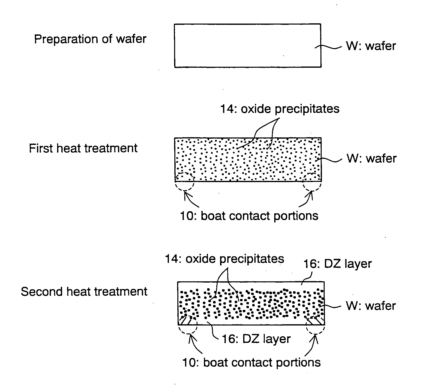
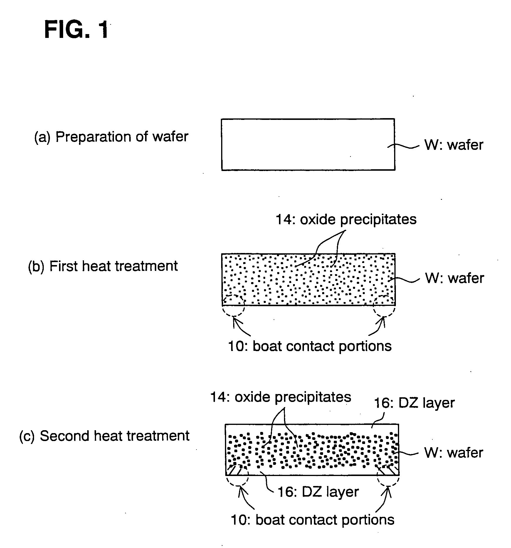
[0035] A diameter of 300 mm, p type, a crystal axis orientation , a resistivity of 10 Ωcm, a nitrogen concentration of 5×10¹³ atoms / cm3, and an initial interstitial oxygen concentration of 14 ppma (values as measured in accordance with Japan Electronic Industry Development Association (JAIDA) standard)<

800° C., 4 hr+1000° C., 16 hr; a 100% argon atmosphere

1200° C., 1 hr; a 100% argon atmosphere

1) Observation of slip dislocations is performed by the X-ray topographic method.

[0036] 2) A DZ layer and an oxide precipitate density are measured by observation under an optical microscope of a wafer etched with a preferential etching solution containing no hexa-valent chromium ion according to a testing method of crystal defects in silicon by preferential etching method priscribed in Japanese Industrial Standard (JIS H 0609:1999) after angle polishing.

[0037] The wafer above described was subjected to the first heat treatment and the second heat treatment under the above-mentioned con...

example 2

A diameter of 300 mm, p type, a crystal axis orientation , a resistivity of 10 Ωcm, undoped with nitrogen, and an initial interstitial oxygen concentration of 16 ppma

700° C., 4 hr+1000° C., 8 hr; a nitrogen atmosphere with an oxygen concentration of 3%<

1150° C., 4 hr; a 100% argon atmosphere

[0039] The first heat treatment and the second heat treatment were applied to the wafer under the above-mentioned conditions, then slip dislocations, a DZ layer and an oxide precipitate density were measured in a similar way as in Example 1, and results of the measurements are shown in Table 1. As shown in Table 1, in Example 2, no generation of slip dislocations in the wafer was observed, a DZ layer with a sufficient width was formed in a surface layer section thereof and an oxide precipitate density in the bulk thereof was sufficiently high.


PUM

PropertyMeasurementUnit
temperatureaaaaaaaaaa
diameteraaaaaaaaaa

Abstract

There are provided a heat-treating method capable of suppressing generation of slip in a CZ silicon single crystal wafer having a diameter of mainly 300 mm or more even under high temperature heat treatment to annihilate grown-in defects in the vicinity of a surface of the wafer, and an annealed wafer having a DZ layer in a surface layer of the wafer and oxide precipitates in the bulk thereof at a high density which exert a high gettering effect. First heat treatment of a silicon single crystal wafer manufactured from a silicon single crystal ingot pulled by means of a Czochralski method is performed at a temperature in the range of 600 to 1100° C. to form oxide precipitates in the bulk of the wafer, and thereafter, second heat treatment is performed at a temperature in the range of 1150 to 1300° C.

Description

RELATED APPLICATION [0001] This application is a continuation application of patent application Ser. No. 10 / 220,145, filed on Aug. 28, 2002, now pending, which application is a national stage of Application No. PCT / JP01 / 10846 filed on Dec. 11, 2001.TECHNICAL FIELD [0002] The present invention relates to a manufacturing process for an annealed wafer in which a silicon single crystal wafer (hereinafter may be simply referred to as a wafer) having mainly a large diameter of 300 mm or more is heat-treated, and an annealed wafer obtained by the manufacturing process. BACKGROUND ART [0003] With the progress of high integration and high functionality of a semiconductor device using a silicon single crystal wafer, the silicon single crystal wafer used in device fabrication is becoming larger in diameter. At present, a 200 mm (8-inch) wafer is a main current of the kinds of wafer, but it is expected that a 300 mm wafer will advance into quantity production and in the near future the 300 mm w...

Claims


Application Information

Patent Timeline
Patent Type & Authority Applications(United States)
IPC IPC(8): B32B13/04H01L21/324C30B29/06H01L21/322
CPCH01L21/3225H01L21/324
Inventor HAYAMIZU, YOSHINORITOBE, SATOSHIKOBAYASHI, NORIHIRO
Owner SHIN-ETSU HANDOTAI CO LTD
Why Eureka
Try Eureka