

Recessed gate for an image sensor
a technology of image sensor and recessed gate, which is applied in the direction of electrical equipment, semiconductor devices, radio frequency controlled devices, etc., can solve the problems of performance variability, reducing the efficiency and dynamic range of the gate, and controlling so as to improve the control of the readout of charge, eliminate any potential barrier interference, and improve the effect of fill factor
- Summary
- Abstract
- Description
- Claims
- Application Information
AI Technical Summary
Benefits of technology
Problems solved by technology
Method used
Image

Examples
Embodiment Construction
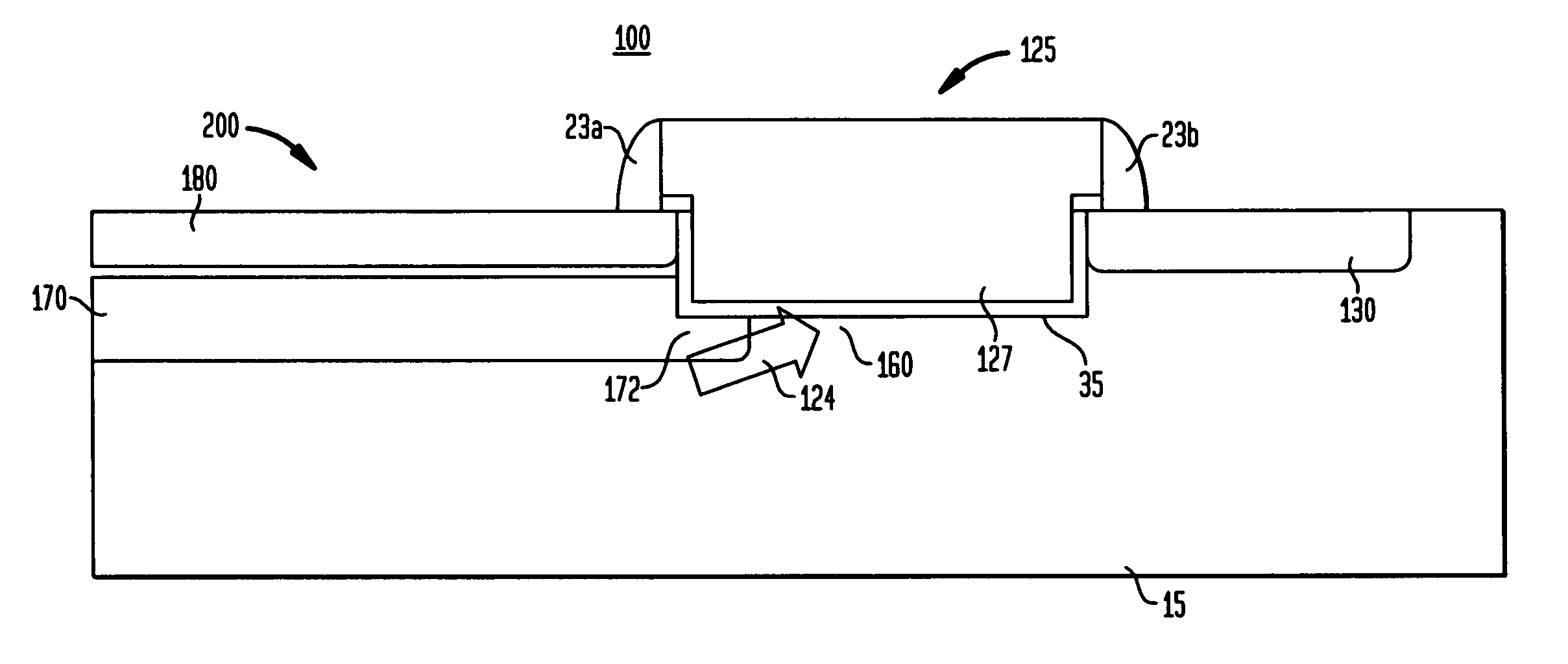
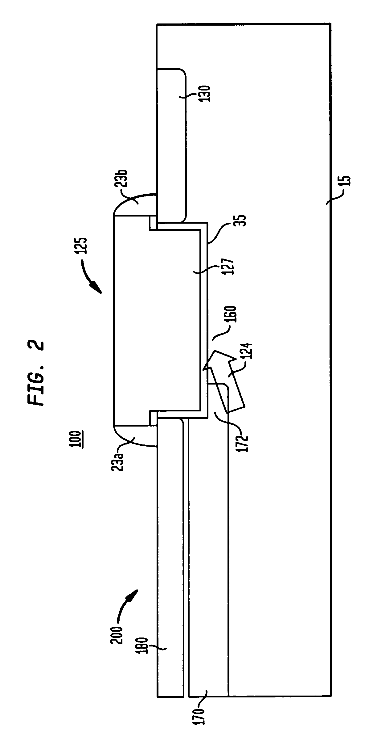
[0026]FIG. 2 illustrates the image sensor APS cell 100 of the present invention. As shown in FIG. 2, the APS cell 100 includes a transfer gate 125 formed on top of a gate dielectric material layer 35 which is formed on top of a semiconductor substrate 15 having a recessed portion 127 formed below the substrate surface. Abutting one side of the transfer gate is a photodiode 200 comprising a surface pinning layer 180 doped with material of a first conductivity, e.g., p type material dopant, and an charge collection well 170 doped with material of a second conductivity, e.g., n type material dopant, formed directly underneath the pinning layer.
[0027] Abutting the other side of the transfer gate is a gate diffusion region 130 comprising doped with material of a second conductivity, e.g., n type material dopant. As shown in FIG. 2, the transfer gate channel 160 formed underneath the transfer gate 125 intersects a portion 172 of the subsequently formed abutting charge collection well reg...
PUM
 Abstract
Description
Claims
Application Information