

Low-Cost Deep Trench Decoupling Capacitor Device and Process of Manufacture
a capacitor and trench decaping technology, applied in the field of trench decapping capacitors, can solve the problem that the process is the least expensive, and achieve the effect of increasing the cost of the base (non-edram) wafer, reducing the number of processes to fabricate the “shallow” trench decaping, and increasing flexibility
- Summary
- Abstract
- Description
- Claims
- Application Information
AI Technical Summary
Benefits of technology
Problems solved by technology
Method used
Image

Examples
first embodiment
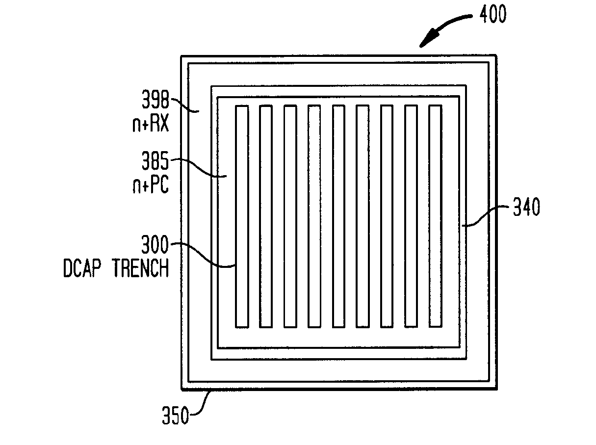
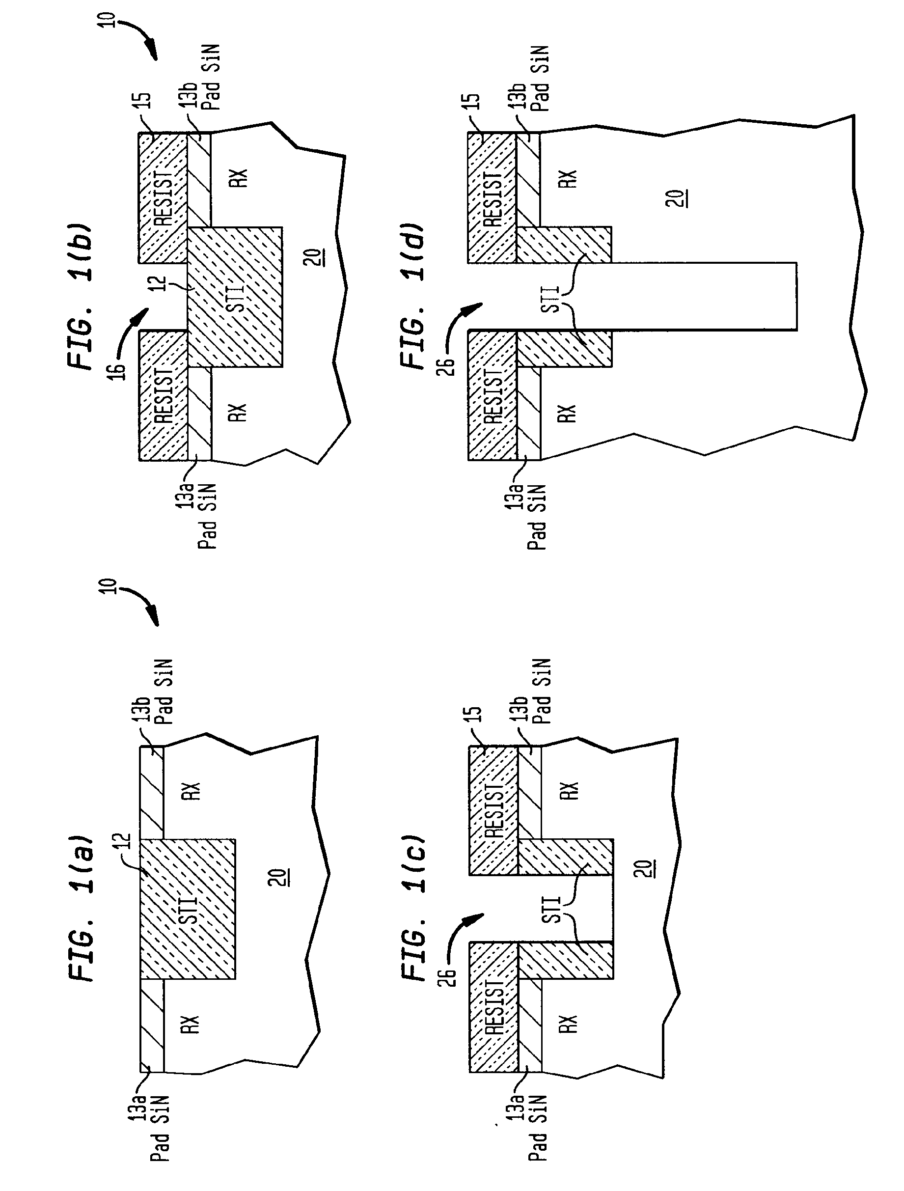
[0025] In accordance with the first embodiment described herein with respect to FIGS. 1(a)-1(i), the only additional costs beyond the POR cost is cost of the additional mask needed to form the decap trench and the cost of performing the associated process steps of opening the DT mask open etch, the DT RIE step, the node process and the N+ polyfill deposition, CMP and recess steps.
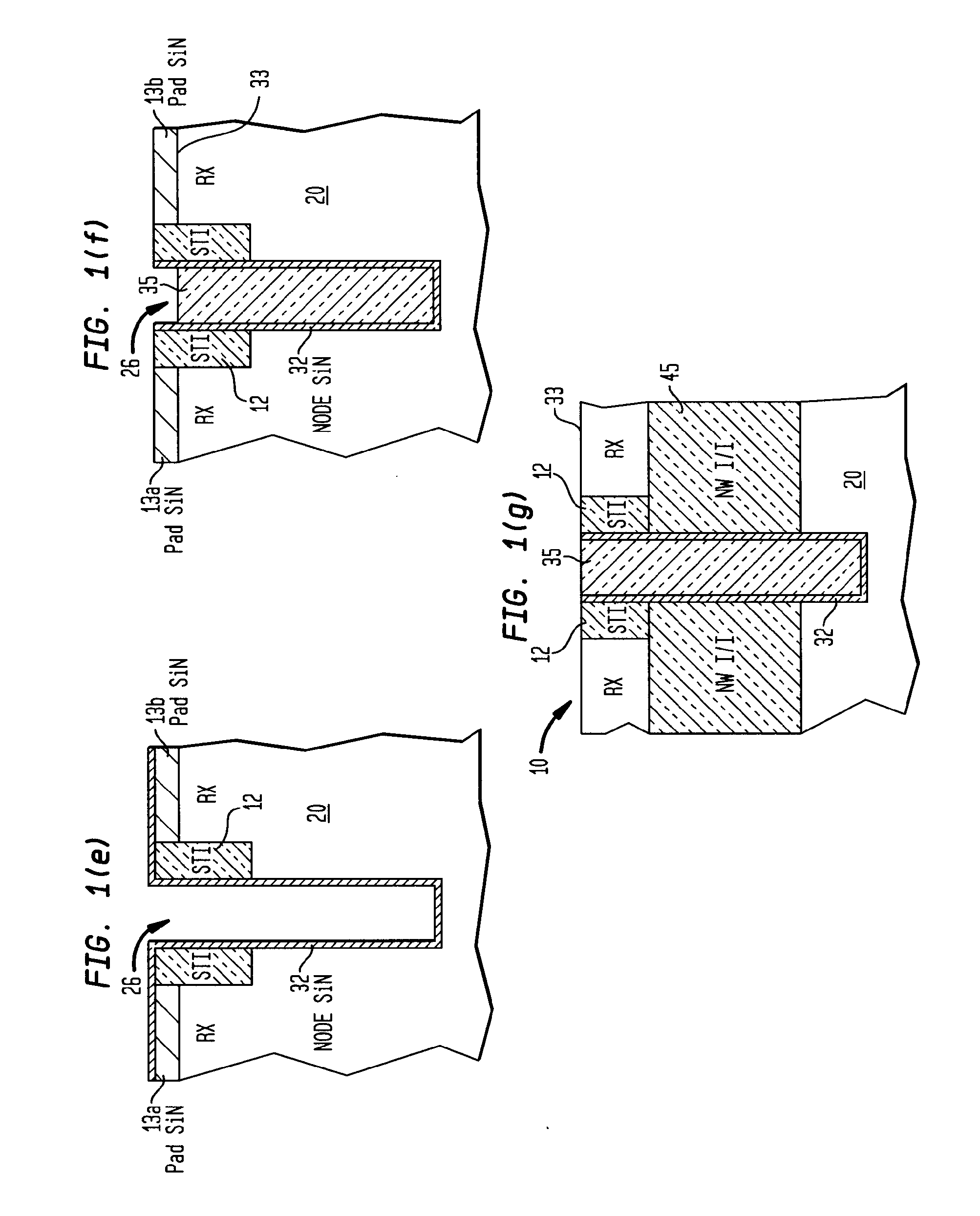
[0026] Because the N-well formed is lightly doped, under certain bias conditions, a depletion region may form that affects the performance of the device. For example, if the N-well (forming the outer decap electrode) is at ground and the inner decap electrode (trench) is at a positive voltage, a depletion region forms that may affect another device, e.g., PFET area nearby, because of the depletion formed in the N-well. Rather than enforcing a ground rule, which would increase the device area, the solution in accordance with the second embodiment is now described. In this second embodiment, the sidewalls of ...
second embodiment
[0027] Thus, after the trench has been lithographically defined and etched as shown in process steps described herein with respect to FIGS. 1(a)-1(d) are performed, as shown in FIG. 2(a)(i)-2(a)(iii), there are several ways that a thin, heavily-doped N-type diffusion layer may be provided in the “shallow” trench decaps. One method of doping the sidewalls of the trench is to perform an angled implant of dopant, e.g., P or As. For example, as shown in FIG. 2(a)(i), dopant ions 60 may be implanted in the trench sidewalls 27 at an angle of incidence of, for example, 5 degrees or less angle from normal incidence, depending on the depth of the trench. A second method, as shown in FIG. 2(a)(ii), utilizes a gas-phase doping process whereby the open DT trench 26 is exposed to high concentration P or As gases 61. A third method, as shown in FIG. 2(a)(iii) is to simply fill the trenches with a doped gas 62, e.g., ASG (arsenic silicate glass) or PSG (phosphorus silicate glass) material layers, ...
third embodiment
[0030] The low-cost decoupling capacitor according to further embodiments of the invention is now described herein with respect to FIGS. 3 and 4. In the third embodiment, the trench decaps are made at a lower cost, exhibit higher frequency response while lowering the overall leakage of a decap design and lowering the area set aside for decaps and, are integrated into an silicon-on-insulator (SOI) designs. There are two distinct “low-cost” trench decap structures and process variations described: a first variation described herein with respect to FIGS. 3(a)-3(j) depicts a process flow where the trench decap design is quickly and seamlessly integrated into an existing SOI technology process. The process calls for an additional two (2) masks: a DT mask and a block-level N-well mask such that the outer plate of the trench decap can be contacted through existing substrate contacts for SOI (e.g., doped poly contacts). In the second variation process described herein with respect to FIGS. ...
PUM
 Abstract
Description
Claims
Application Information