Vertical double-diffused metal oxide semiconductor (VDMOS) device incorporating reverse diode

a metal oxide semiconductor and reverse diode technology, applied in semiconductor devices, diodes, electrical devices, etc., can solve the problems of vdmos whose endurance to esd and eos is weakened, and cannot endure eos and esd, so as to prevent a breakdown

Inactive Publication Date: 2006-06-15
SAMSUNG ELECTRONICS CO LTD
View PDF13 Cites 22 Cited by
  • Summary
  • Abstract
  • Description
  • Claims
  • Application Information

AI Technical Summary

Benefits of technology

[0013] Exemplary embodiments according to the invention are directed to a DMOS device which is able to prevent a breakdown from a strong current stress such as ESD or EOD.
[0014] Some exemplary embodiments according to the invention provide a DMOS device which prevents a strong current from being concentrated on a portion that cannot endure a current stress by redistributing the strong current momentarily generated.
[0017] A gate electrode of the DMOS device according to the present invention is overlapped with a part of the source region. A channel of a MOS transistor is defined in the body region of the second conductivity type of the second diffusion structure by the gate electrode. A threshold voltage of the MOS transistor is lower than a turn-on voltage of the bipolar transistor, and a turn-on voltage of the bipolar transistor is lower than a reverse breakdown voltage of the diode. Due to theses characteristics, the breakdown of the DMOS device can be prevented under a normal operation voltage and with the occurrence of a strong current such as ESD or EOD, when for example a high-power DMOS transistor with a channel formed in the body region is operatedand a bipolar transistor is operated in the source region sufficiently isolated from the drain region.

Problems solved by technology

The VDMOS occupies a smaller area compared to the LDMOS, but cannot endure EOS and ESD.
As a result of a low doping concentration of the source and drain regions, a current crowding induced by base push-out phenomenon occurs, thereby bringing about a thermal breakdown of the device.
Consequently, a stronger snapback occurs in a lower voltage than a normal voltage, resulting in an VDMOS whose endurance to ESD and EOS is weakened.
In the event that a doping concentration of the source region is low, to have high operation voltage range, a current crowding is induced by a base push-out, and a thermal breakdown of the DMOS device occurs.

Method used


Image

  • Vertical double-diffused metal oxide semiconductor (VDMOS) device incorporating reverse diode
  • Vertical double-diffused metal oxide semiconductor (VDMOS) device incorporating reverse diode
  • Vertical double-diffused metal oxide semiconductor (VDMOS) device incorporating reverse diode

Examples


Embodiment Construction

[0026] The exemplary embodiments of the present invention now will be described more fully hereinafter with reference to the accompanying drawings, in which embodiments of the invention are shown. However, this invention should not be construed as limited to the embodiments set forth herein. In the drawings, the thickness of layers and regions are exaggerated for clarity. Like numbers refer to like elements throughout. It will be understood that when an element such as a layer, region or substrate is referred to as being “on” or extending “onto” another element, it can be directly on or extend directly onto the other element or intervening elements may also be present. Moreover, the term “heavily doped” used herein refers to a higher than average concentration. Like numbers refer to like elements throughout the specification.

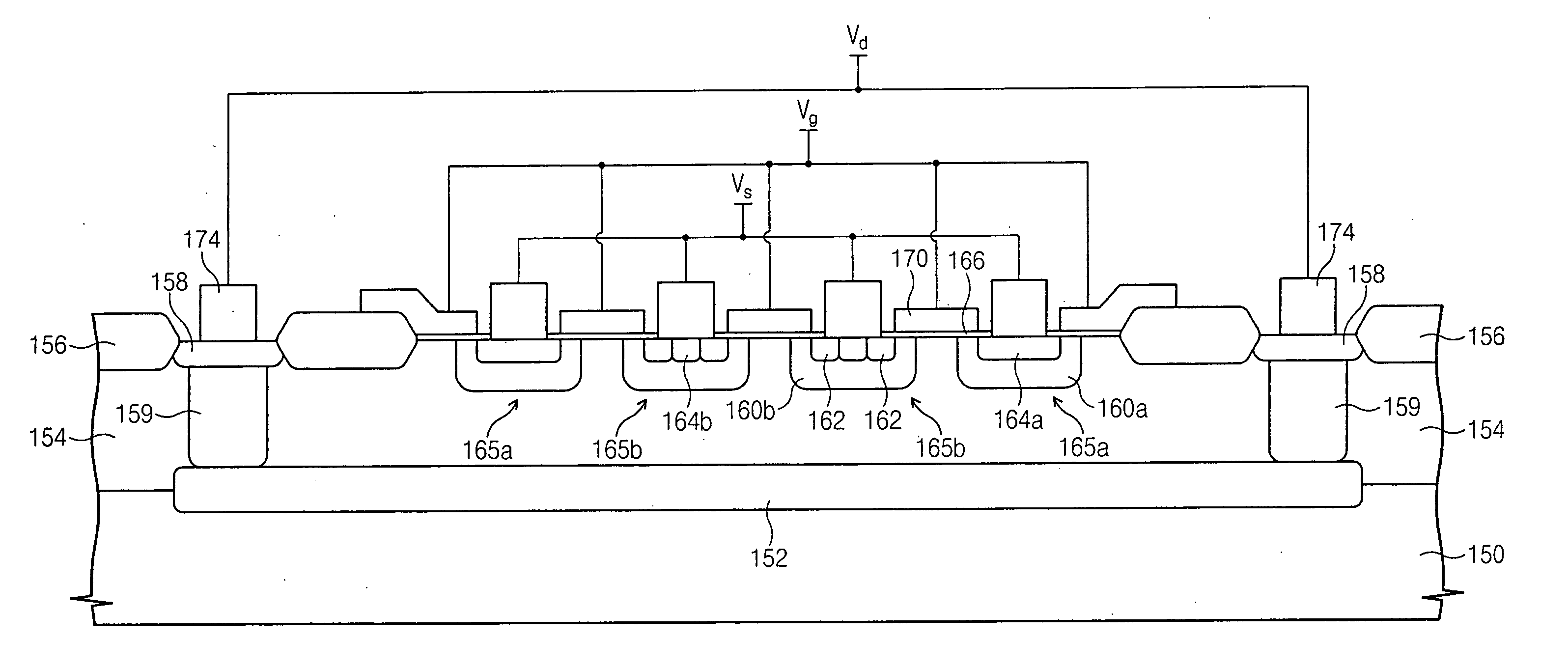
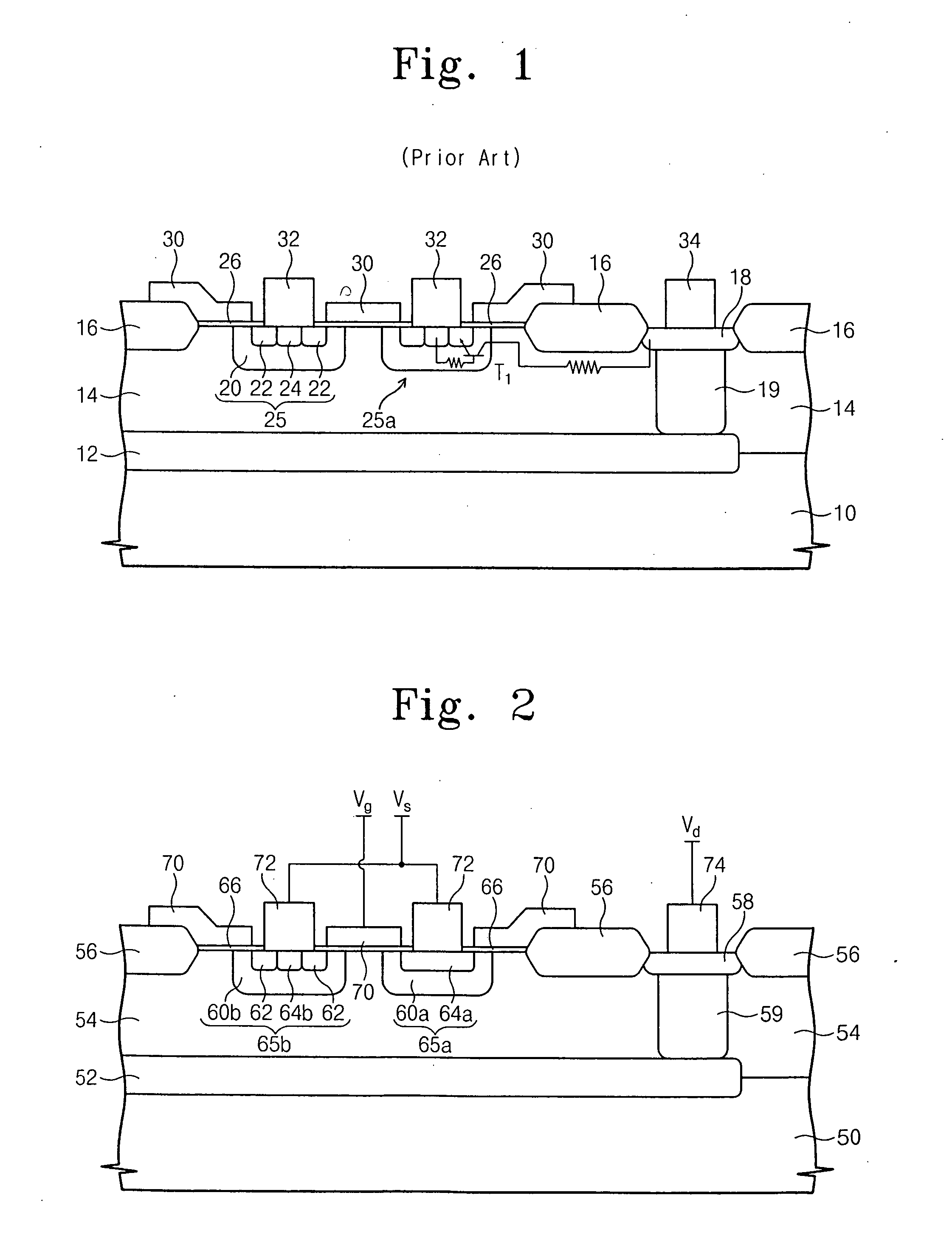
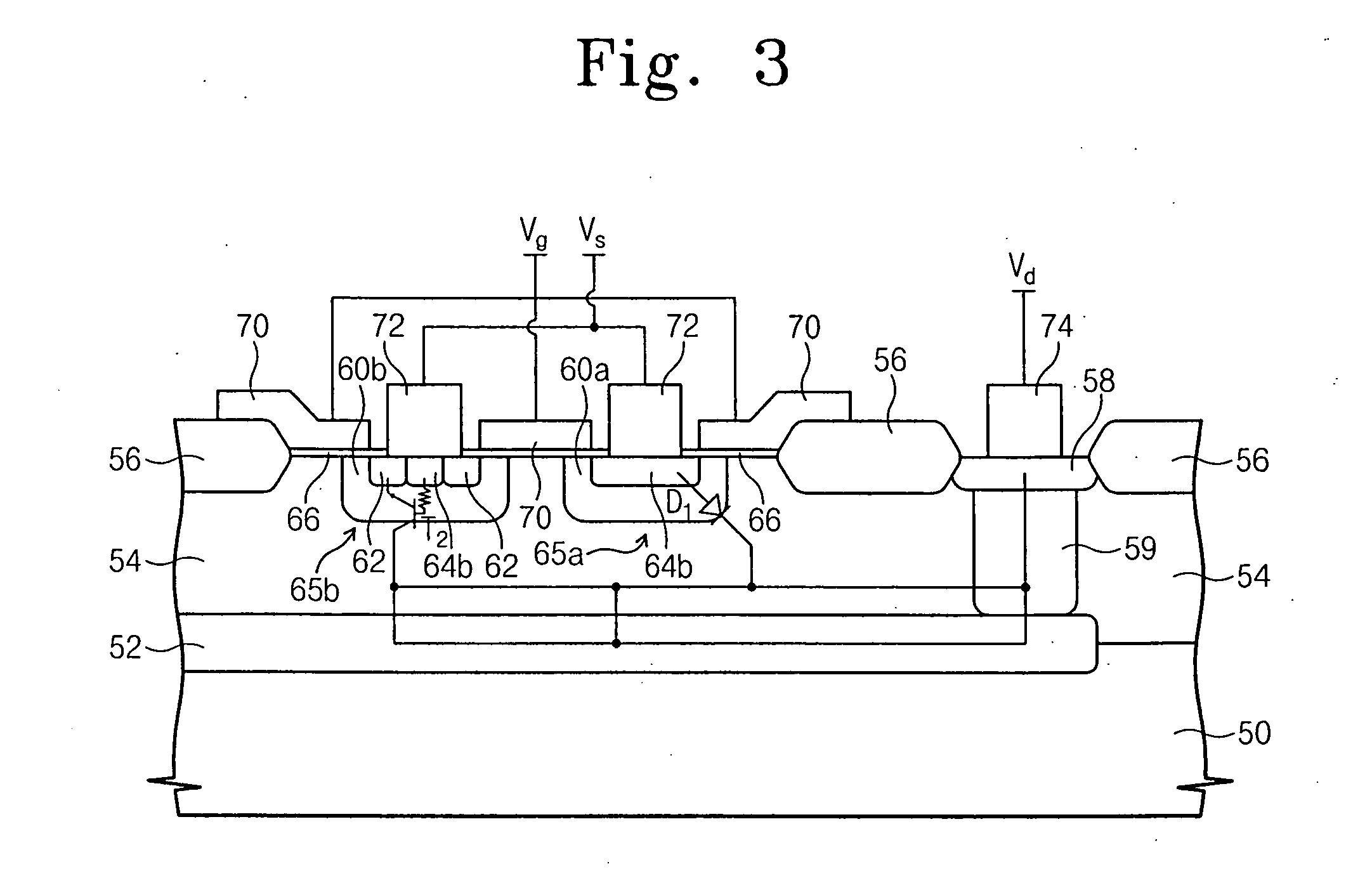
[0027]FIG. 2 shows a VDMOS device according to a preferred embodiment of the present invention.

[0028] With reference to FIG. 2, the VDMOS includes an epitaxia...


PUM


Abstract

The present invention disclosed herein is a Vertical Double-Diffused Metal Oxide Semiconductor (VDMOS) device incorporating a reverse diode. This device includes a plurality of source regions isolated from a drain region. A source region in close proximity to the drain region is a first diffusion structure in which a heavily doped diffusion layer of a second conductivity type is formed in a body region of a second conductivity type. Another source region is a second diffusion structure in which a heavily doped diffusion layer of a first conductivity type and a heavily doped diffusion layer of the second conductivity type are formed in the body region of the second conductivity type. An impurity diffusion structure of the source region in close proximity to the drain region is changed to be operated as a diode, thereby forming a strong current path to ESD (Electro-Static Discharge) or EOS (Electrical Over Stress). As a result, it is possible to prevent the device from being broken down.

Description

[0001] This application claims priority from Korean Patent Application No. 2004-106393, filed on Dec. 15, 2004, the contents of which is herein incorporated by reference in its entirety. [0002] 1. Field of the Invention [0003] This invention generally relates to Double Diffused Metal Oxide Semiconductor (DMOS) devices and, more specifically, to a vertical DMOS device having a strong endurance to EOS (Electrical Over Stress) and ESD (Electrical-Static Discharge) with a reverse diode. [0004] 2. Background of the Invention [0005] DMOS devices are high-voltage devices with low power consumption and high speed. The DMOS devices are classified into Lateral Double-Diffused Metal Oxide Semiconductor (LDMOS) and Vertical Double-Diffused Metal Oxide Semiconductor (VDMOS). The VDMOS occupies a smaller area compared to the LDMOS, but cannot endure EOS and ESD. [0006] A DMOS device with an operation voltage higher than several volts increases a breakdown voltage by doping a source region and a d...

Claims


Application Information

Patent Timeline
Patent Type & Authority Applications(United States)
IPC IPC(8): H01L29/76
CPCH01L29/42368H01L29/7805H01L29/7809H01L29/781
Inventor JANG, SUNG-PILKIM, HAN-GUJEON, CHAN-HEE
Owner SAMSUNG ELECTRONICS CO LTD
Why Eureka
Try Eureka