

Method for manufacturing semiconductor device
- Summary
- Abstract
- Description
- Claims
- Application Information
AI Technical Summary
Benefits of technology
Problems solved by technology
Method used
Image

Examples
embodiment mode 1
[0057] Embodiment mode of the present invention is hereinafter described with reference to drawings. It is to be understood by those of skilled in the art that the invention can be applied in various modes, and the mode and the detail can be variously changed unless it departs from the content and the scope of the invention. The invention is not limited to the description of this embodiment mode.
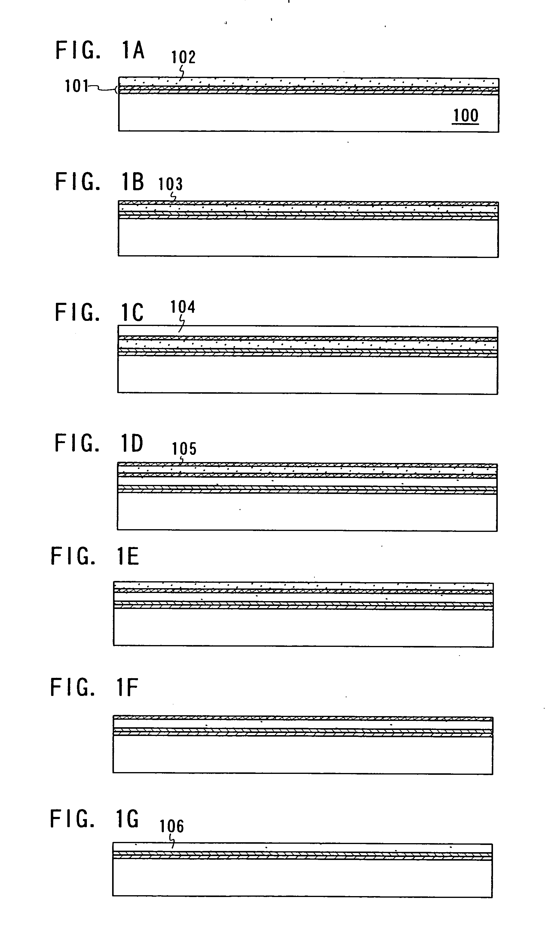
[0058] In this embodiment, a method for preventing holes from being generated on a surface of a crystalline silicon film in the case of removing an etching stopper composed of a silicon oxide film formed on the surface of the crystalline silicon film during guttering, and a natural oxide film (silicon oxide film) formed on a gettering site composed of an amorphous silicon film formed on the etching stopper is described with reference to FIGS. 1A to 1G.
[0059] First, an amorphous silicon film is formed after forming a base insulating film 101 over a substrate 100 and crystallized using an el...
embodiment mode 2
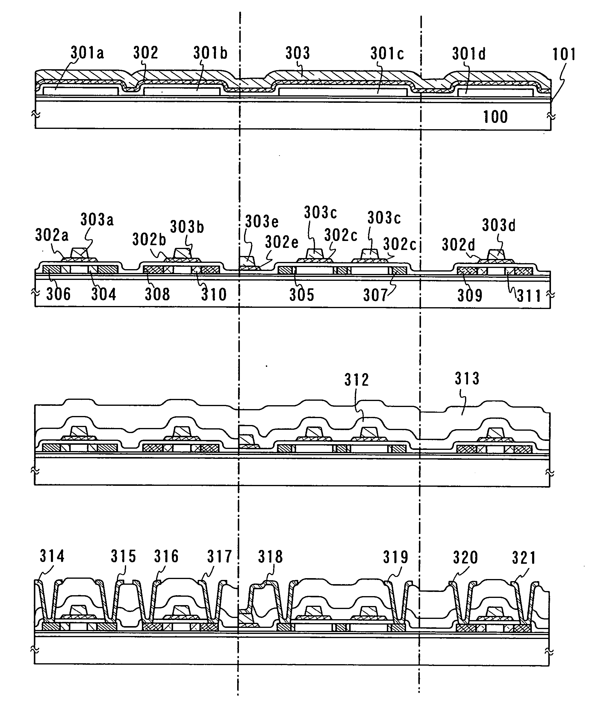
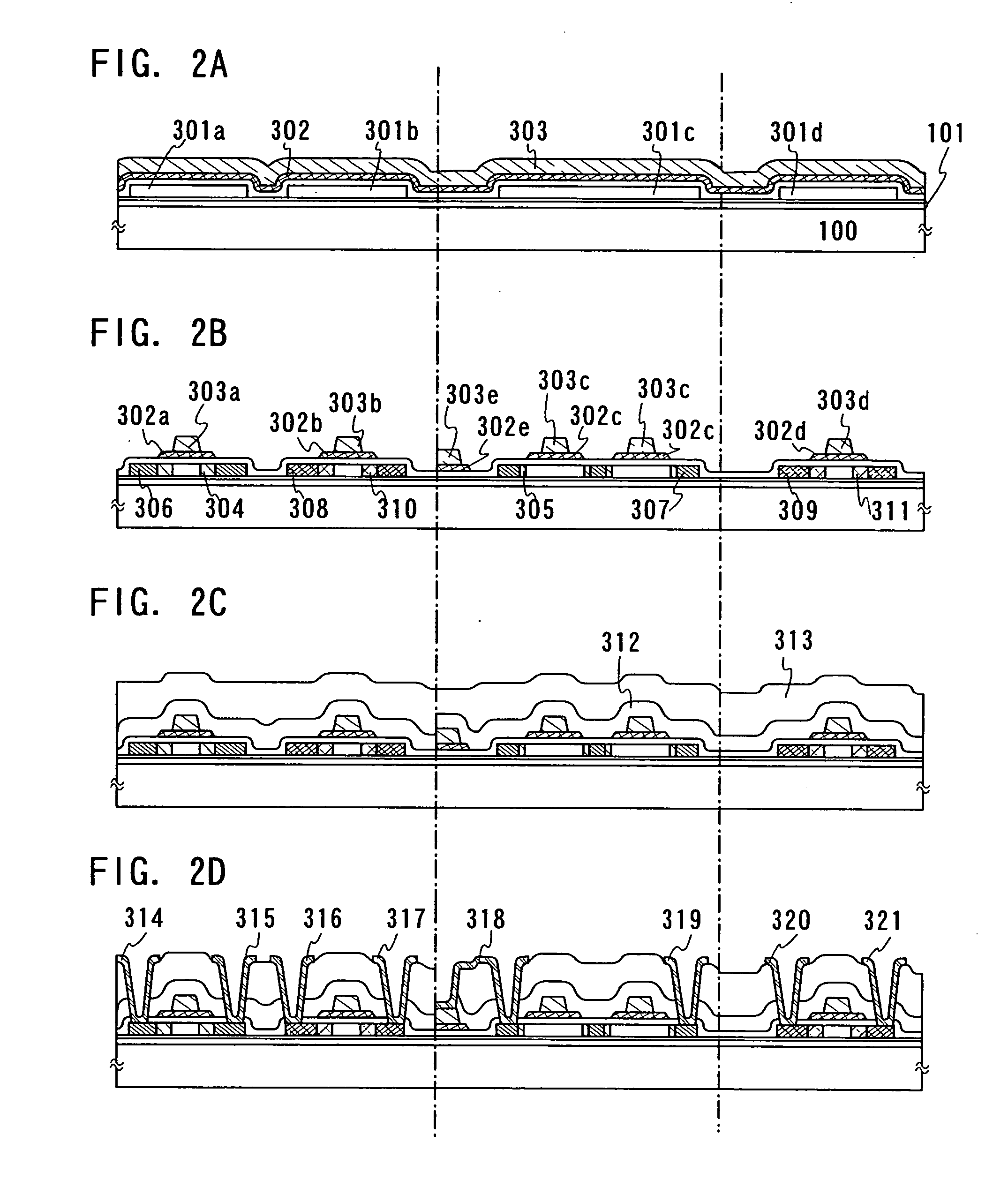
[0088] In this embodiment mode, a method for manufacturing a thin film transistor and a capacitor according to the present invention is described with reference to FIG. 2A to 2D.
[0089] First, a small amount of impurities for controlling a threshold depending on necessity is doped in the crystalline silicon film 106 obtained in Embodiment Mode 1, which is also referred to as channel doping. In order to obtain the required threshold, boron, phosphorus, or the like is doped by ion doping or the like.
[0090] Then, crystalline silicon films 301a to 301d each having island shapes are obtained by patterning into predetermined shape as shown in FIG. 2A. The patterning is performed by applying a photoresist to the crystalline silicon film; exposing to be the predetermined mask shape; baking; forming a mask over the crystalline semiconductor film; and etching the crystalline silicon film using the mask by dry etching. CF4, O2, and the like are used as gases in dry etching.
[0091] Subsequentl...
example 1
[0129] In this example, an example of forming a light emitting device using a thin film transistor and a capacitor manufactured according to the present invention is described with reference to FIG. 3.
[0130] In the light emitting device described in this example, a layer including a substance which emits light is sandwiched between a pair of electrodes, and an element which emits light by flowing current between the electrodes is arranged in a matrix form. It is assumed that emission mechanism of a light emitting element is as follows: by applying voltage between a pair of electrodes while sandwiching an organic compound layer therebetween, electron injected from a cathode and a hole injected from an anode are recombined at the center of the light emission to form a molecular exciton, and energy is discharged to emit light when the molecular exciton returns to the ground state.
[0131] The excitation state is known to include a singlet excitation and a triplet excitation, and it is ...
PUM
 Abstract
Description
Claims
Application Information